- 您現在的位置:買賣IC網 > PDF目錄374022 > ADP3604* (Analog Devices, Inc.) Dual/Quad Rail-to-Rail Output, Picoamp Input Precision Op Amps; Package: SO; No of Pins: 8; Temperature Range: -40°C to +85°C PDF資料下載
參數資料
| 型號: | ADP3604* |
| 廠商: | Analog Devices, Inc. |
| 英文描述: | Dual/Quad Rail-to-Rail Output, Picoamp Input Precision Op Amps; Package: SO; No of Pins: 8; Temperature Range: -40°C to +85°C |
| 中文描述: | 開關電容電壓轉換器,具有穩壓輸出 |
| 文件頁數: | 7/8頁 |
| 文件大小: | 143K |
ADP3604
REV. 0
–7–
POWE R DISSIPAT ION
T he power dissipation of the ADP3604 circuit must be limited
such that the junction temperature of the device does not ex-
ceed the maximum junction temperature rating.
Power is dissipated in two components, power loss due to volt-
age drops in the switches, and the power loss due to MOSFET
drive current losses. T otal power dissipation is calculated:
P
≈
(
V
IN
– |
V
OU
T
|)(
I
OUT
) + (
V
IN
)(
I
S
)
where both
V
IN
and
V
OUT
are referred to ground pin of the
ADP3604.
For example: Assuming the worst case conditions, V
IN
= 5.5 V,
V
OUT
= –2.8 V, and I
OUT
= 120 mA, calculated power dissipa-
tion is:
P
≈
(5.5
V
–|–2.8
V
|)(0.12) + (5.5
V
)(0.003
A
) = 341
mW
T his is far below the power dissipation capability of the
ADP3604 package which is 660 mW.
LAY OUT AND GROUNDING T IPS
T he ADP3604 switches turn on and off very fast. Good PC
board layout practices will ensure the proper operation of the
device. Important layout considerations include:
Use adequate ground and power traces or planes.
K eep components as close as possible to the device.
Use short trace lengths from the input and output capacitors to
the input and output pins respectively.
Use single point ground for the device ground pins and the in-
put and output capacitors.
Improper layouts will result in poor load regulation, especially
with heavy loads.
APPLICAT IONS
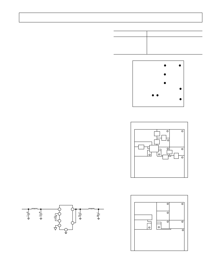
ADP3604 E VALUAT ION BOARD LAY OUT
T he ADP3604 evaluation board is a general purpose circuit
board. Its flexible design allows the user to optimize the circuit
performance by external components selection and circuit con-
figuration. T he circuit board can be configured as a basic charge
pump voltage inverter with one pump capacitor and two bypass
capacitors or as a more complex circuit with input and output
LC filters.
PC layout is designed for surface mount components and can
be easily configured for through hole components as well.
ADP3604
8
7
3
C3
4.7μF
1
4
V
IN
+4.5 – +6V
V
OUT
–3.0V
C4
4.7μF
2
5
SENSE
INPUT
L2
10μH
C5
4.7μF
C2
4.7μF
L1
1μH
C1
4.7μF
Figure 21. Evaluation Board Circuit Diagram
C2
C1
C4
C5
L1
C3
L2
Figure 23. Eight-Pin SOIC-Layout, Component Placement
Diagram (1
×
Scale)
Figure 24. Eight-Pin-SOIC Layout, Component Side
(1
×
Layout)
T able V. Recommended Components for Circuit in Figure 21
Component
Manufacturer/T ype
C3
C1, C2, C4, C5
L1
L2
Sprague, 293D475X 0035D2W
T OK IN, 1E475ZY5UC205F
Coiltronics, CT X 32CT -1R0
Coiltronics, CT X 32CT -100
FILTERED INPUT
INPUT
OUTPUT
FILTERED OUTPUT
SHDN
OUTPUT GND
Figure 22. Eight-Pin SOIC Layout, Wiring Connection
相關PDF資料 |
PDF描述 |
|---|---|
| ADP3605ARU-3 | 120 mA Switched Capacitor Voltage Inverter with Regulated Output |
| ADP3605AR-3 | 120 mA Switched Capacitor Voltage Inverter with Regulated Output |
| ADP3605AR | Secondary Over-Voltage Protection for 2-4 cell in series Li-Ion/Poly (4.45V) 8-SM8 -40 to 110 |
| ADP3605 | 120 mA Switched Capacitor Voltage Inverter with Regulated Output(穩壓輸出的開關電容電壓反相器) |
| ADP3607ARU-5 | 50 mA Switched Capacitor Voltage Boost with Regulated Output |
相關代理商/技術參數 |
參數描述 |
|---|---|
| ADP3604AR | 制造商:Rochester Electronics LLC 功能描述:SW CAPACITOR VOLT CONV W/REG OUTPUT - Bulk |
| ADP3604AR-REEL | 制造商:Analog Devices 功能描述: |
| ADP3605 | 制造商:AD 制造商全稱:Analog Devices 功能描述:120 mA Switched Capacitor Voltage Inverter with Regulated Output |
| ADP36050001RUR | 制造商:Analog Devices 功能描述: |
發布緊急采購,3分鐘左右您將得到回復。