- 您現在的位置:買賣IC網 > PDF目錄374023 > ADP3605 (Analog Devices, Inc.) 120 mA Switched Capacitor Voltage Inverter with Regulated Output(穩壓輸出的開關電容電壓反相器) PDF資料下載
參數資料
| 型號: | ADP3605 |
| 廠商: | Analog Devices, Inc. |
| 元件分類: | 基準電壓源/電流源 |
| 英文描述: | 120 mA Switched Capacitor Voltage Inverter with Regulated Output(穩壓輸出的開關電容電壓反相器) |
| 中文描述: | 120毫安開關電容電壓逆變器(穩壓輸出的開關電容電壓反相器和穩壓輸出) |
| 文件頁數: | 6/8頁 |
| 文件大小: | 218K |
| 代理商: | ADP3605 |
ADP3605
–6–
REV. 0
Pump Capacitor
The ADP3605 alternately charges C
P
to the input voltage when
C
P
is switched in parallel with the input supply, and then trans-
fers charge to C
O
when C
P
is switched in parallel with C
O
.
During the time C
P
is charging, the peak current is approxi-
mately two times the output current.
During the time C
P
is delivering charge to C
O
, the supply cur-
rent drops down to about 3 mA.
A low ESR capacitor has much greater impact on performance
for C
P
than C
O
since current through C
P
is twice the C
O
cur-
rent. Therefore, the voltage drop due to C
P
is about four times
the ESR of C
P
times the load current. While the ESR of C
O
affects the output ripple voltage, the voltage drop generated by
the ESR of C
P
, combined with the voltage drop due to the output
source resistance, determines the maximum available V
OUT
.
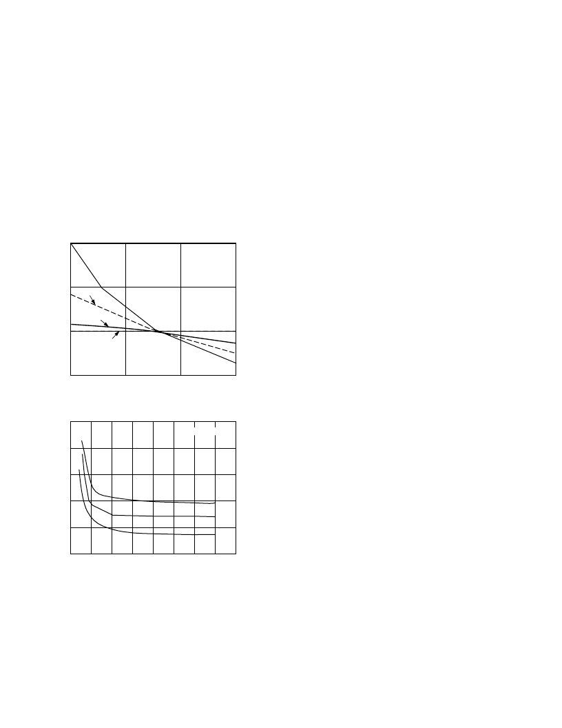
TEMPERATURE –
8
C
10
1.0
0.01–50
100
0
E
V
50
0.1
ALUMINUM
CERAMIC
TANTALUM
ORGANIC SEMIC
Figure 13. ESR vs. Temperature
CAPACITANCE –
m
F
100
80
00
160
20
O
40
60
80
100
120
140
60
40
20
ADP3605-3
150m
V
100m
V
50m
V
Figure 14. Output Ripple Voltage (mV) vs. Capacitance
and ESR
Improved Load Regulation
In most applications, the IR drop from printed circuit board
traces is not critical. V
SENSE
should be connected to the output
at a convenient PCB location close to the load. However, if a
reduction in IR drop or improvement in load regulation is de-
sired, the sense line can be used to monitor the output voltage
at the load. To avoid excessive noise pickup, keep the V
SENSE
line as short as possible and away from any noisy line.
Shutdown Mode
The ADP3605’s output can be disabled by pulling the SD pin
(Pin 4) high to a TTL/CMOS logic compatible level which will
stop the internal oscillator. In shutdown mode, the quiescent
current is reduced to 2
μ
A (typical). Applying a digital low level
or tying the SD Pin to ground will turn on the output. If the
shutdown feature is not used, Pin 4 should be tied to the
ground pin.
Power Dissipation
The power dissipation of the ADP3605 circuit must be limited
such that the junction temperature of the device does not exceed
the maximum junction temperature rating. Total power dissipa-
tion is calculated as follows:
P
= (
V
IN
–|
V
OUT
|)
I
OUT
+ (
V
IN
)
I
S
Where
I
OUT
and
I
S
are output current and supply current,
V
IN
and
V
OUT
are input and output voltages respectively.
For example: assuming worst case conditions, V
IN
= 6 V,
V
OUT
= –2.9 V, I
OUT
= 120 mA and I
S
= 5 mA. Calculated
device power dissipation is:
P
≈
(6
V
–|–2.9
V
|)(0.12) + (6
V
)(0.005
A
) = 402
mW
This is far below the 660 mW power dissipation capability of the
ADP3605 in SO-8 or 600 mW in RU-14
General Board Layout Guidelines
Since the ADP3605’s internal switches turn on and off very fast,
good PC board layout practices are critical to ensure optimal
operation of the device. Improper layouts will result in poor load
regulation, especially under heavy loads. Following these simple
layout guidelines will improve output performance.
1. Use adequate ground and power traces or planes.
2. Use single point ground for device ground and input and
output capacitor grounds.
3. Keep external components as close to the device as possible.
4. Use short traces from the input and output capacitors
to the input and output pins respectively.
相關PDF資料 |
PDF描述 |
|---|---|
| ADP3607ARU-5 | 50 mA Switched Capacitor Voltage Boost with Regulated Output |
| ADP3607AR | Secondary Over-Voltage Protection for 2-4 cell in series Li-Ion/Poly (4.45V) 8-TSSOP -40 to 110 |
| ADP3607ARU | Secondary Over-Voltage Protection for 2-4 cell in series Li-Ion/Poly (4.45V) 8-TSSOP -40 to 110 |
| ADP3607AR-5 | 50 mA Switched Capacitor Voltage Boost with Regulated Output |
| ADP3607 | 50 mA Regulated Output Switched Capacitor Voltage Doubler.(50mA 調節電流輸出,轉換比較器電壓倍增器) |
相關代理商/技術參數 |
參數描述 |
|---|---|
| ADP36050001RUR | 制造商:Analog Devices 功能描述: |
| ADP3605AR | 制造商:Analog Devices 功能描述:Charge Pump INV -3V to -6V 120mA 8-Pin SOIC N 制造商:Analog Devices 功能描述:IC VOLTAGE REGULATOR |
| ADP3605AR-3 | 制造商:Analog Devices 功能描述:Charge Pump INV -3V 120mA 8-Pin SOIC N |
| ADP3605AR-3-REEL | 制造商:Analog Devices 功能描述:Charge Pump INV -3V 120mA 8-Pin SOIC N T/R |
| ADP3605AR-REEL | 制造商:Analog Devices 功能描述:Charge Pump INV -3V to -6V 120mA 8-Pin SOIC N T/R |
發布緊急采購,3分鐘左右您將得到回復。