- 您現在的位置:買賣IC網 > PDF目錄374023 > ADP3605AR (ANALOG DEVICES INC) Secondary Over-Voltage Protection for 2-4 cell in series Li-Ion/Poly (4.45V) 8-SM8 -40 to 110 PDF資料下載
參數資料
| 型號: | ADP3605AR |
| 廠商: | ANALOG DEVICES INC |
| 元件分類: | 穩壓器 |
| 英文描述: | Secondary Over-Voltage Protection for 2-4 cell in series Li-Ion/Poly (4.45V) 8-SM8 -40 to 110 |
| 中文描述: | SWITCHED CAPACITOR REGULATOR, 288 kHz SWITCHING FREQ-MAX, PDSO8 |
| 封裝: | SOIC-8 |
| 文件頁數: | 7/8頁 |
| 文件大小: | 197K |
| 代理商: | ADP3605AR |
ADP3605
–7–
REV. A
Maximum Output Voltage
Maximum unregulated output voltage can be obtained on the
ADP3605-3 by connecting the V
SENSE
pin to ground instead of
to the V
OUT
pin. Under this condition, the magnitude of the
unregulated output voltage depends on the load current. V
OUT
is inversely proportional to the load current as illustrated in
Figure 15.
LOAD CURRENT – mA
–5.0
–3.0
0
120
V
O
20
40
60
80
100
–4.0
ADP3605-3
V
IN
= +5.0V
Figure 15. Maximum Unregulated Output Voltage
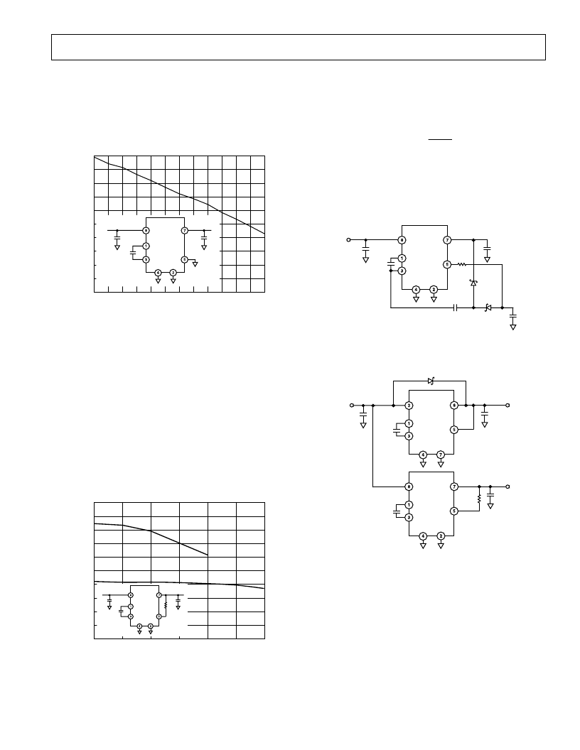
Regulated Adjustable Output Voltage
For the adjustable version of the ADP3605, the regulated out-
put voltage is programmed by a resistor which is inserted be-
tween the V
SENSE
and V
OUT
pins, as illustrated in Figure 16.
The inherent limit of the output voltage of a single inverting
charge pump stage is –1 times the input voltage. The inverse
(i.e., negative) scaling factor of 1.00 is reduced somewhat due to
losses that increase with output current. To increase the scaling
factor to attain a more negative output voltage, an external
pump stage can be added with just passive components as
shown in Figure 17. That single stage increases the inverse
scaling factor to a limit of two, although the diode drops will
limit the ability to attain that exact 2.00 scaling factor notice-
ably. Even further increases can be achieved with more external
pump stages.
LOAD CU60
–5.0
–3.0
0
120
V
O
20
40
80
100
–4.0
ADP3605
V
IN
= +5.0V
V
OUT
R
R = 29k
V
R = 24k
V
Figure 16. Adjustable Regulated Output Voltage
High accuracy on the adjustable output voltage is achieved with
the use of precision trimmed internal resistors, which eliminates
the need to trim the external resistor or add a second resistor to
form a divider. The adjustable output voltage is set using the
following formula:
V
OUT
=
–
1.5
9.5
k
R
where
V
OUT
is in volts and
R
is in k
.
Regulated Dual Supply System
The circuit in Figure 18 provides regulated positive and negative
voltages for systems that require dual supplies from a single
battery or power supply.
ADP3605
V
IN
C
P
+
C
P
–
SD
V
SENSE
V
OUT
GND
+
C
P
4.7
m
F
C
IN
4.7
m
F
V
IN
= +5V
C
O
4.7
m
F
+
+10
m
F
C1
4.7
m
F
D2
1N5817
D1
1N5817
+
+
R1
44.2k
V
Figure 17. Regulated –7 V from a 5 V Input
ADP3607-5
V
IN
C
P
+
C
P
–
SD
V
SENSE
V
OUT
GND
+
C
P1
10
m
F
10
m
F
C
O1
10
m
F
+
+
+5V
ADP3605
V
IN
C
P
+
C
P
–
SD
V
SENSE
V
OUT
GND
+
C
P2
10
m
F
C
O2
10
m
F
+
R1
16.5k
V
1%
1N5817
V
IN
= +3.3V
–2.6V
Figure 18. Dual Supply System
相關PDF資料 |
PDF描述 |
|---|---|
| ADP3605 | 120 mA Switched Capacitor Voltage Inverter with Regulated Output(穩壓輸出的開關電容電壓反相器) |
| ADP3607ARU-5 | 50 mA Switched Capacitor Voltage Boost with Regulated Output |
| ADP3607AR | Secondary Over-Voltage Protection for 2-4 cell in series Li-Ion/Poly (4.45V) 8-TSSOP -40 to 110 |
| ADP3607ARU | Secondary Over-Voltage Protection for 2-4 cell in series Li-Ion/Poly (4.45V) 8-TSSOP -40 to 110 |
| ADP3607AR-5 | 50 mA Switched Capacitor Voltage Boost with Regulated Output |
相關代理商/技術參數 |
參數描述 |
|---|---|
| ADP3605AR-3 | 制造商:Analog Devices 功能描述:Charge Pump INV -3V 120mA 8-Pin SOIC N |
| ADP3605AR-3-REEL | 制造商:Analog Devices 功能描述:Charge Pump INV -3V 120mA 8-Pin SOIC N T/R |
| ADP3605AR-REEL | 制造商:Analog Devices 功能描述:Charge Pump INV -3V to -6V 120mA 8-Pin SOIC N T/R |
| ADP3605ARU-3 | 制造商:AD 制造商全稱:Analog Devices 功能描述:120 mA Switched Capacitor Voltage Inverter with Regulated Output |
| ADP3605ARU-3-REEL | 制造商:Analog Devices 功能描述:Charge Pump INV -3V 120mA 14-Pin TSSOP T/R 制造商:Rochester Electronics LLC 功能描述:120MA SWITCHED CAPACITOR VOLT. REGULATOR - Tape and Reel |
發布緊急采購,3分鐘左右您將得到回復。