- 您現在的位置:買賣IC網 > PDF目錄374024 > ADR03CRZ2 (Analog Devices, Inc.) Ultracompact Precision10 V/5 V/2.5 V/3.0 V Voltage References PDF資料下載
參數資料
| 型號: | ADR03CRZ2 |
| 廠商: | Analog Devices, Inc. |
| 英文描述: | Ultracompact Precision10 V/5 V/2.5 V/3.0 V Voltage References |
| 中文描述: | 超小型Precision10第V / 5 V/2.5 V/3.0 V電壓參考 |
| 文件頁數: | 17/20頁 |
| 文件大小: | 837K |
| 代理商: | ADR03CRZ2 |
ADR01/ADR02/ADR03/ADR06
To optimize the resolution of this circuit, dual-supply op amps
should be used because the ground potential of ADR02 can
swing from –5 V at zero scale to V
L
at full scale of the potenti-
ometer setting.
Rev. F | Page 17 of 20
PROGRAMMABLE 4 TO 20 mA CURRENT
TRANSMITTER
Because of their precision, adequate current handling, and small
footprint, the devices are suitable as the reference sources for
many high performance converter circuits. One of these
applications is the multichannel 16-bit 4 to 20 mA current
transmitter in the industrial control market (see Figure 42). This
circuit employs a Howland current pump at the output, which
yields better efficiency, a lower component count, and a higher
voltage compliance than the conventional design with op amps
and MOSFETs. In this circuit, if the resistors are matched such
that R1 = R1
′
, R2 = R2
′
, R3 = R3
′
, the load current is
R
)
R
(R
I
2
3
′
N
REF
L
D
V
R
1
3
2
×
×
+
=
(2)
where
D
is similarly the decimal equivalent of the DAC input
code and
N
is the number of bits of the DAC.
According to Equation 2, R3
′
can be used to set the sensitivity.
R3
′
can be made as small as necessary to achieve the current
needed within U4 output current driving capability. On the
other hand, other resistors can be kept high to conserve power.
U1
15V
V
IN
V
OUT
GND
TEMP TRIM
U1 = ADR01/ADR02/ADR03/ADR06, REF01
U2 = AD5543/AD5544/AD5554
U3, U4 = AD8512
U2
5V
10V
+15V
–15V
V
DD
V
REF
GND
RF
IO
IO
AD5544
DIGITAL INPUT
CODE 20%–100% FULL SCALE
U3
V
X
0V TO –10V
R1
150k
R2
15k
U4
C1
10pF
VP
R3
50
AD8512
R3'
50
V
L
R1'
150k
LOAD
500
4–20mA
VN
V
O
R2'
15k
0
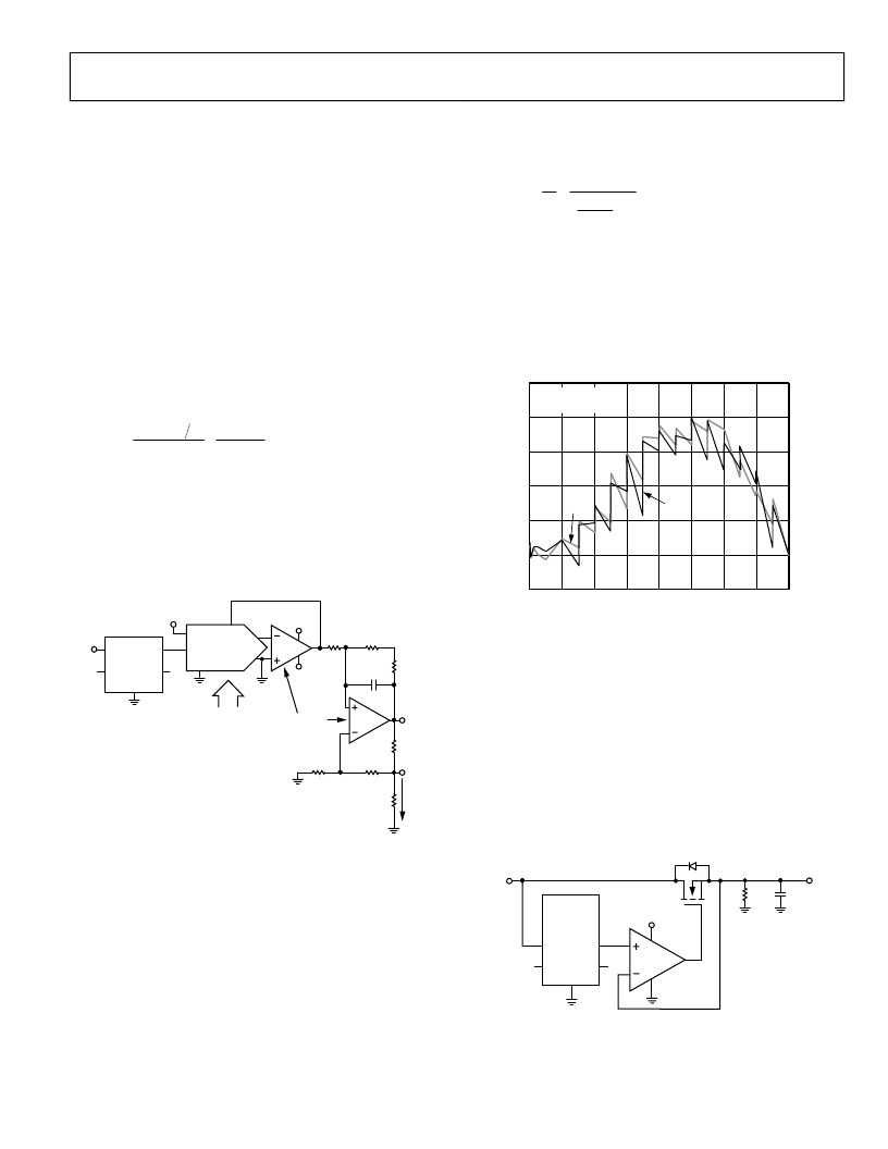
Figure 42. Programmable 4 to 20 mA Transmitter
In this circuit, the AD8512 is capable of delivering 20 mA of
current, and the voltage compliance approaches 15 V.
The Howland current pump yields a potentially infinite output
impedance, which is highly desirable, but resistance matching is
critical in this application. The output impedance can be deter-
mined using Equation 3. As can be seen by this equation, if the
resistors are perfectly matched, Z
O
is infinite. On the other hand,
if they are not matched, Z
O
is either positive or negative. If the
latter is true, oscillation may occur. For this reason, a capacitor, C1,
in the range of 1 pF to 10 pF should be connected between VP
and the output terminal of U4, to filter any oscillation.
′
=
=
1
R1R2
′
′
R2
R1
R1
I
V
Z
t
t
O
(3)
In this circuit, an ADR01 provides the stable 10.000 V reference
for the AD5544 quad 16-bit DAC. The resolution of the adjust-
able current is 0.3 μA/step, and the total worst-case INL error is
merely 4 LSB. Such error is equivalent to 1.2 μA or a 0.006%
system error, which is well below most systems’ requirements.
The result is shown in Figure 43 with measurement taken at 25°C
and 70°C; total system error of 4 LSB at both 25°C and 70°C.
5
–1
0
65536
8192
16384
24576
32768
40960
49152
57344
4
3
2
1
0
CODE (Decimal)
I
R
L
= 500
I
L
= 0mA TO 20mA
25
o
C
70
o
C
0
Figure 43. Result of Programmable 4 to 20 mA Current Transmitter
Precision Boosted Output Regulator
A precision voltage output with boosted current capability can
be realized with the circuit shown in Figure 44. In this circuit,
U2 forces V
O
to be equal to V
REF
by regulating the turn-on of
N1, thereby making the load current furnished by V
IN
. In this
configuration, a 50 mA load is achievable at V
IN
of 15 V. Moderate
heat is generated on the MOSFET, and higher current can be
achieved with a replacement of a larger device. In addition, for a
heavy capacitive load with a fast edging input signal, a buffer
should be added at the output to enhance the transient response.
U2
15V
N1
200
U1
ADR01/
ADR02/
ADR03/
ADR06
V
IN
V
OUT
TEMP TRIM
GND
V–
V+
OP1177
2N7002
V
IN
V
O
R
L
1
μ
F
C
L
0
Figure 44. Precision Boosted Output Regulator
相關PDF資料 |
PDF描述 |
|---|---|
| ADR06 | Ultracompact Precision10 V/5 V/2.5 V/3.0 V Voltage References |
| ADR01BR-REEL7 | Ultracompact Precision10 V/5 V/2.5 V/3.0 V Voltage References |
| ADR01BUJ-R2 | Ultracompact Precision10 V/5 V/2.5 V/3.0 V Voltage References |
| ADR01BUJ-REEL7 | Ultracompact Precision10 V/5 V/2.5 V/3.0 V Voltage References |
| ADR01CRZ-REEL2 | Ultracompact Precision10 V/5 V/2.5 V/3.0 V Voltage References |
相關代理商/技術參數 |
參數描述 |
|---|---|
| ADR03CRZ-REEL | 制造商:Analog Devices 功能描述: |
| ADR03CRZ-REEL2 | 制造商:AD 制造商全稱:Analog Devices 功能描述:Ultracompact Precision10 V/5 V/2.5 V/3.0 V Voltage References |
| ADR03NBC | 制造商:Analog Devices 功能描述: |
| ADR03WARZ-R7 | 功能描述:IC VREF SERIES PREC 2.5V 8SOIC RoHS:是 類別:集成電路 (IC) >> PMIC - 電壓基準 系列:- 產品培訓模塊:Voltage Reference Basics 標準包裝:100 系列:- 基準類型:旁路,精度 輸出電壓:4.096V 容差:±0.075% 溫度系數:50ppm/°C 輸入電壓:- 通道數:1 電流 - 陰極:1µA 電流 - 靜態:- 電流 - 輸出:10mA 工作溫度:0°C ~ 70°C 安裝類型:表面貼裝 封裝/外殼:8-SOIC(0.154",3.90mm 寬) 供應商設備封裝:8-SOIC 包裝:管件 |
| ADR03WARZ-RL | 功能描述:IC VREF SERIES PREC 2.5V 8SOIC RoHS:是 類別:集成電路 (IC) >> PMIC - 電壓基準 系列:- 產品培訓模塊:Voltage Reference Basics 標準包裝:100 系列:- 基準類型:旁路,精度 輸出電壓:4.096V 容差:±0.075% 溫度系數:50ppm/°C 輸入電壓:- 通道數:1 電流 - 陰極:1µA 電流 - 靜態:- 電流 - 輸出:10mA 工作溫度:0°C ~ 70°C 安裝類型:表面貼裝 封裝/外殼:8-SOIC(0.154",3.90mm 寬) 供應商設備封裝:8-SOIC 包裝:管件 |
發布緊急采購,3分鐘左右您將得到回復。