- 您現在的位置:買賣IC網 > PDF目錄374025 > ADR291ER-RELL (Analog Devices, Inc.) Low Noise Micropower Precision Voltage References PDF資料下載
參數資料
| 型號: | ADR291ER-RELL |
| 廠商: | Analog Devices, Inc. |
| 英文描述: | Low Noise Micropower Precision Voltage References |
| 中文描述: | 低噪聲微精密電壓基準 |
| 文件頁數: | 12/15頁 |
| 文件大小: | 199K |
| 代理商: | ADR291ER-RELL |
REV. B
ADR290/ADR291/ADR292
–12–
Device Power Dissipation Considerations
The ADR29x family of references is guaranteed to deliver load
currents to 5 mA with an input voltage that ranges from 2.7 V
to 15 V (minimum supply voltage depends on output voltage
option). When these devices are used in applications with large
input voltages, care should be exercised to avoid exceeding the
published specifications for maximum power dissipation or junc-
tion temperature that could result in premature device failure.
The following formula should be used to calculate a device
’
s maxi-
mum junction temperature or dissipation:
P
T
T
D
A
A
=
J
J
–
θ
In this equation,
T
J
and
T
A
are the junction and ambient tem-
peratures, respectively,
P
D
is the device power dissipation, and
θ
J
A
is the device package thermal resistance.
Basic Voltage Reference Connections
References, in general, require a bypass capacitor connected
from the V
OUT
pin to the GND pin. The circuit in Figure 2
illustrates the basic configuration for the ADR29x family of ref-
erences. Note that the decoupling capacitors are not required for
circuit stability.
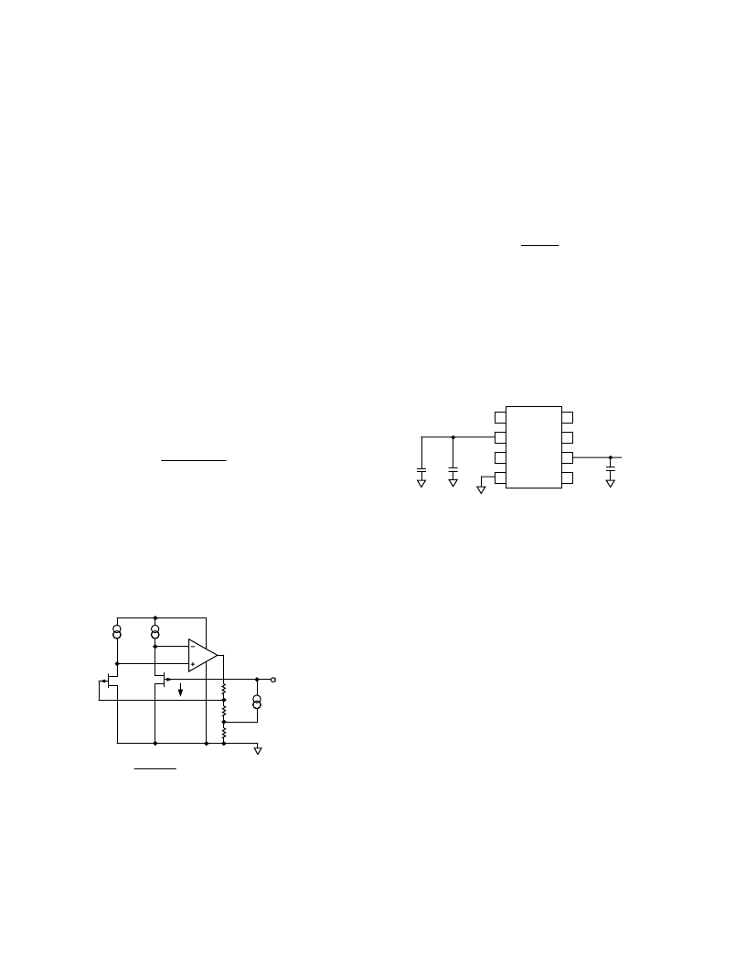
ADR29x
1
2
3
4
8
7
6
5
NC
NC
NC
NC
OUTPUT
NC
0.1 F
0.1 F
10 F
+
NC = NO CONNECT
Figure 2. Basic Voltage Reference Configuration
Noise Performance
The noise generated by the ADR29x family of references is typi-
cally less than 12
μ
V p-p over the 0.1 Hz to 10 Hz band. TPC
21 shows the 0.1 Hz to 10 Hz noise of the ADR290 which is only
6
μ
V p-p. The noise measurement is made with a bandpass filter
made of a 2-pole high-pass filter with a corner frequency at 0.1 Hz
and a 2-pole low-pass filter with a corner frequency at 10 Hz.
Turn-On Time
Upon application of power (cold start), the time required for the
output voltage to reach its final value within a specified error band
is defined as the turn-on settling time. Two components nor-
mally associated with this are the time for the active circuits to
settle, and the time for the thermal gradients on the chip to sta-
bilize. TPC 28 shows the turn-on settling time for the ADR291.
THEORY OF OPERATION
The ADR29x series of references uses a new reference generation
technique known as XFET (eXtra implanted junction FET). This
technique yields a reference with low noise, low supply current
and very low thermal hysteresis.
The core of the XFET reference consists of two junction field-
effect transistors, one of which has an extra channel implant to
raise its pinch-off voltage. By running the two JFETs at the
same drain current, the difference in pinch-off voltage can be
amplified and used to form a highly stable voltage reference.
The intrinsic reference voltage is around 0.5 V with a negative
temperature coefficient of about
–
120 ppm/K. This slope is
essentially locked to the dielectric constant of silicon and can be
closely compensated by adding a correction term generated in
the same fashion as the proportional-to-temperature (PTAT)
term used to compensate bandgap references. The big advantage
over a bandgap reference is that the intrinsic temperature coeffi-
cient is some thirty times lower (therefore less correction is
needed) and this results in much lower noise since most of the
noise of a bandgap reference comes from the temperature com-
pensation circuitry.
The simplified schematic below shows the basic topology of the
ADR29x series. The temperature correction term is provided by
a current source with value designed to be proportional to abso-
lute temperature. The general equation is:
V
V
R
R
R
R
I
R
OUT
P
PTAT
=
+
+
+
(
)(
)
1
2
1
3
3
where
V
P
is the difference in pinch-off voltage between the two
FETs, and
I
PTAT
is the positive temperature coefficient correc-
tion current. The various versions of the ADR29x family are
created by on-chip adjustment of R1 and R3 to achieve 2.048 V,
2.500 V or 4.096 V at the reference output.
The process used for the XFET reference also features vertical
NPN and PNP transistors, the latter of which are used as output
devices to provide a very low drop-out voltage.
V
OUT
V
IN
I
PTAT
GND
R1
R2
R3
I
1
I
1
*
*
EXTRA
CHANNEL
IMPLANT
V
OUT
=R1
+
R2
+
R3
R1
V
P
+ I
PTAT
R3
V
P
Figure 1. ADR290/ADR291/ADR292 Simplified Schematic
相關PDF資料 |
PDF描述 |
|---|---|
| ADR291FR-RELL | Low Noise Micropower Precision Voltage References |
| ADR291GR-REEL | Low Noise Micropower Precision Voltage References |
| ADR291GR-REEL7 | Low Noise Micropower Precision Voltage References |
| ADR291GR-RELL | Low Noise Micropower Precision Voltage References |
| ADR291GRU-RELL | Low Noise Micropower Precision Voltage References |
相關代理商/技術參數 |
參數描述 |
|---|---|
| ADR291ERZ | 功能描述:IC VREF SERIES PREC 2.5V 8-SOIC RoHS:是 類別:集成電路 (IC) >> PMIC - 電壓基準 系列:XFET® 標準包裝:3,000 系列:- 基準類型:旁路,精度 輸出電壓:3V 容差:±0.5% 溫度系數:100ppm/°C 輸入電壓:- 通道數:1 電流 - 陰極:82µA 電流 - 靜態:- 電流 - 輸出:15mA 工作溫度:-40°C ~ 85°C 安裝類型:表面貼裝 封裝/外殼:6-TSSOP(5 引線),SC-88A,SOT-353 供應商設備封裝:SC-70-5 包裝:帶卷 (TR) 其它名稱:296-20888-2 |
| ADR291ERZ | 制造商:Analog Devices 功能描述:IC SERIES V-REF 2.5V 2mV 8-SOIC 制造商:Analog Devices 功能描述:IC, SERIES V-REF, 2.5V, 2mV, 8-SOIC |
| ADR291ERZ-REEL7 | 功能描述:IC VREF SERIES PREC 2.5V 8-SOIC RoHS:是 類別:集成電路 (IC) >> PMIC - 電壓基準 系列:XFET® 標準包裝:2,000 系列:- 基準類型:旁路,可調節,精度 輸出電壓:1.24 V ~ 16 V 容差:±0.5% 溫度系數:- 輸入電壓:1.24 V ~ 16 V 通道數:1 電流 - 陰極:100µA 電流 - 靜態:- 電流 - 輸出:20mA 工作溫度:-40°C ~ 85°C 安裝類型:通孔 封裝/外殼:TO-226-3、TO-92-3(TO-226AA)成形引線 供應商設備封裝:TO-92-3 包裝:帶卷 (TR) |
| ADR291FR | 制造商:Analog Devices 功能描述:V-Ref Precision 2.5V 5mA 8-Pin SOIC N Tube 制造商:Rochester Electronics LLC 功能描述:LOW NOISE MICROPWR PRECISION VOLT. REF. - Bulk 制造商:Analog Devices 功能描述:IC VOLT REF |
| ADR291FR-REEL | 制造商:Analog Devices 功能描述:V-Ref Precision 2.5V 5mA 8-Pin SOIC N T/R |
發布緊急采購,3分鐘左右您將得到回復。