- 您現在的位置:買賣IC網 > PDF目錄374026 > ADR318ARJ-REEL7 (ANALOG DEVICES INC) Precision Low Drift SOT-23 Voltage Reference with Shutdown PDF資料下載
參數資料
| 型號: | ADR318ARJ-REEL7 |
| 廠商: | ANALOG DEVICES INC |
| 元件分類: | 基準電壓源/電流源 |
| 英文描述: | Precision Low Drift SOT-23 Voltage Reference with Shutdown |
| 中文描述: | 1-OUTPUT THREE TERM VOLTAGE REFERENCE, 1.8 V, PDSO5 |
| 封裝: | MO-178AA, SOT-23, 5 PIN |
| 文件頁數: | 6/8頁 |
| 文件大小: | 492K |
| 代理商: | ADR318ARJ-REEL7 |
REV. 0
–6–
ADR318
PARAMETER DEFINITIONS
Temperature Coefficient
Temperature coefficient is the change of output voltage with
respect to operating temperature changes, normalized by the
output voltage at 25
°
C. This parameter is expressed in ppm/
°
C,
and can be determined with the following equation:
°
(
25
where:
V
O
(25
°
C
) =
V
O
at 25
°
C
V
O
(
T
1
) =
V
O
at temperature 1
V
O
(
T
2
) =
V
O
at temperature 2
Long Term Stability
Long term stability is the typical shift of output voltage at 25
°
C
on a sample of parts subjected to a test of 1,000 hours at 25
°
C:
( )
[
( )
0
TCV
ppm
C
°
V T
V T
T
)
×
(
V
C
T
O
O
=
–
)
×
2
1
2
1
6
10
–
(1)
V
V
t
V
t
V
ppm
V
t
V
V
t
t
O
O
O
( )
0
O
O
O
O
=
( )
1
]
=
( )
1
×
0
6
10
(2)
where:
V
O
(
t
0
) =
V
O
at 25
°
C at time 0
V
O
(
t
1
) =
V
O
at 25
°
C after 1,000 hours operation at 25
°
C
Thermal Hysteresis
Thermal hystereses is defined as the change of output voltage
after the device is cycled through temperature from +25
°
C to
–40
°
C to +125
°
C and back to +25
°
C. This is a typical value from a
sample of parts put through such a cycle.
V
V
C
°
V
V
ppm
V
C
°
(
V
C
°
V
O
HYS
O
O TC
_
)
25
O
HYS
O
O TC
_
O
_
_
=
(
]
=
)
(
25
[
×
25
10
6
(3)
where:
V
O
(25
°
C
) =
V
O
at 25
°
C
V
O_TC
=
V
O
at 25
°
C after temperature cycle at +25
°
C to –40
°
C
to +125
°
C and back to +25
°
C
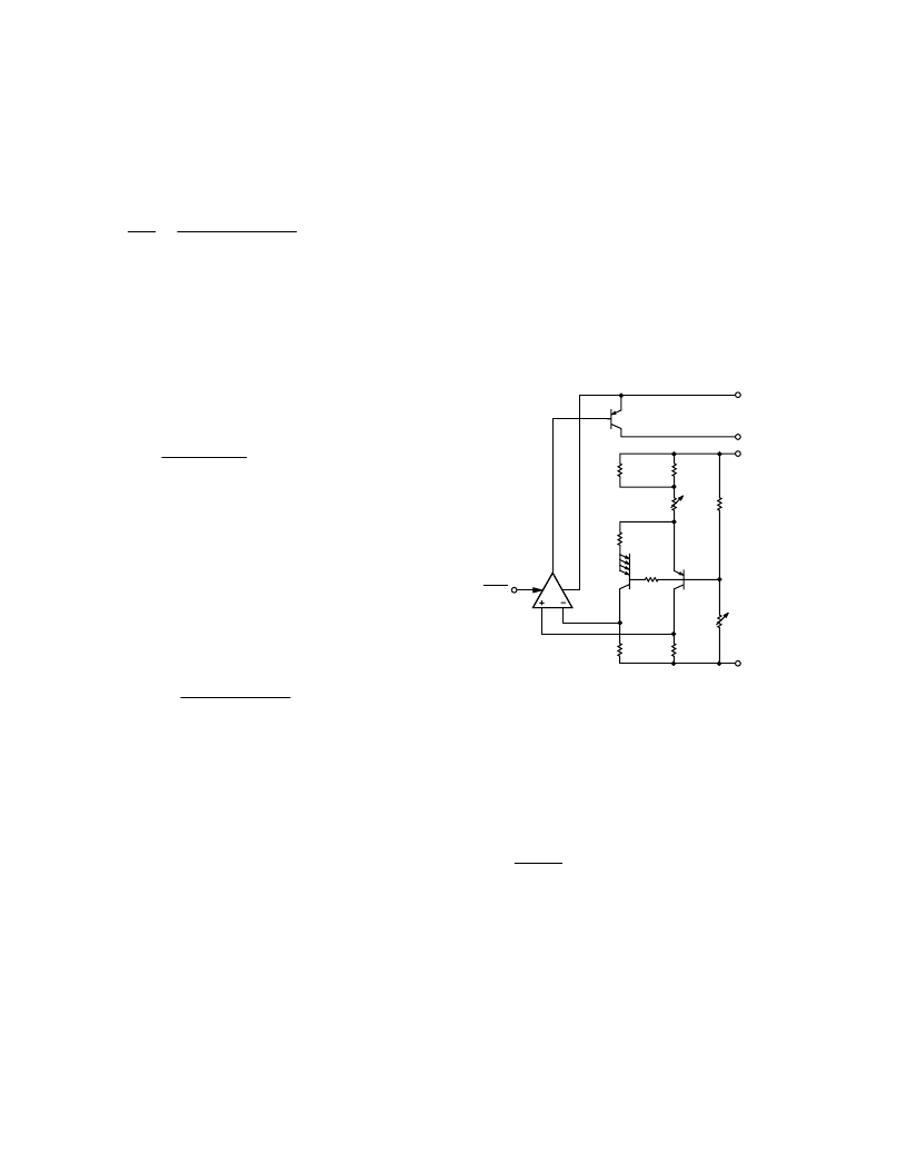
THEORY OF OPERATION
Band gap references are the high performance solution for low
supply voltage and low power voltage reference applications,
and the ADR318 is no exception. The uniqueness of this product
lies in its architecture. By observing Figure 1, the ideal zero TC
band gap voltage is referenced to the output, not to ground.
Therefore, if noise exists on the ground line, it will be greatly
attenuated on V
OUT
. The band gap cell consists of the PNP pair
Q51 and Q52, running at unequal current densities. The difference
in V
BE
results in a voltage with a positive TC that is amplified by
the ratio of 2 R58/R54. This PTAT voltage, combined with
the V
BE
s of Q51 and Q52, produces the stable band gap voltage.
Reduction in band gap curvature is performed by the ratio of
the resistors R44 and R59, one of which is linearly temperature
dependent. Precision laser trimming and other patented circuit
techniques are used to further enhance the drift performance.
SHDN
GND
Q51
R54
R59
Q1
R44
R49
R58
R60
R61
R48
R53
Q52
V
OUT(SENSE)
V
OUT(FORCE)
V
IN
Figure 1. Simplified Schematic
Device Power Dissipation Considerations
The ADR318 is capable of delivering load currents up to 5 mA
with an input voltage that ranges from 2.4 V to 15 V. When this
device is used in applications with high input voltages, care should
be taken to avoid exceeding the specified maximum power dissi-
pation or junction temperature that could result in premature
device failure. The following formula should be used to calculate
the device’s maximum junction temperature or dissipation:
P
T
T
D
A
=
J
JA
θ
(4)
In Equation 4,
T
J
and
T
A
are, respectively, the junction and
ambient temperatures,
P
D
is the device power dissipation, and
θ
JA
is the device package thermal resistance.
Shutdown Mode Operation
The ADR318 includes a shutdown feature that is TTL/CMOS
compatible. A logic LOW or a 0 V condition on the
SHDN
pin
is required to turn the device off. During shutdown, the output
of the reference becomes a high impedance state where its potential
would then be determined by external circuitry. If the shutdown
feature is not used, the
SHDN
pin should be connected to V
IN
(Pin 2).
相關PDF資料 |
PDF描述 |
|---|---|
| ADR363 | Low Power, Low Noise Voltage References with Sink/Source Capability |
| ADR363A | Low Power, Low Noise Voltage References with Sink/Source Capability |
| ADR363AUJZ-REEL7 | Low Power, Low Noise Voltage References with Sink/Source Capability |
| ADR363B | Low Power, Low Noise Voltage References with Sink/Source Capability |
| ADR363BUJZ-REEL7 | Low Power, Low Noise Voltage References with Sink/Source Capability |
相關代理商/技術參數 |
參數描述 |
|---|---|
| ADR318ARJZ-REEL7 | 功能描述:IC VREF SERIES PREC 1.8V SOT23-5 RoHS:是 類別:集成電路 (IC) >> PMIC - 電壓基準 系列:- 標準包裝:1 系列:- 基準類型:串聯,精度 輸出電壓:4.5V 容差:±800µV 溫度系數:1ppm/°C 輸入電壓:13.5 V ~ 22 V 通道數:1 電流 - 陰極:- 電流 - 靜態:7mA 電流 - 輸出:10mA 工作溫度:-55°C ~ 125°C 安裝類型:表面貼裝 封裝/外殼:20-LCC 供應商設備封裝:20-CLCC 包裝:管件 |
| ADR3410 | 制造商:ANADIGICS 制造商全稱:ANADIGICS, Inc 功能描述:50 з High Linearity 1 Watt Amplifier |
| ADR3412 | 制造商:AD 制造商全稱:Analog Devices 功能描述:Micropower, High Accuracy Voltage References |
| ADR3412ARJZ | 制造商:Analog Devices 功能描述:IC VOLT REF 1.25V 6SOT23 制造商:Analog Devices 功能描述:IC, VOLT REF, 1.25V, 6SOT23 |
| ADR3412ARJZ-R2 | 功能描述:IC VREF SERIES PREC 1.2V SOT23-6 RoHS:是 類別:集成電路 (IC) >> PMIC - 電壓基準 系列:- 產品培訓模塊:Voltage Reference Basics 標準包裝:100 系列:- 基準類型:旁路,精度 輸出電壓:4.096V 容差:±0.075% 溫度系數:50ppm/°C 輸入電壓:- 通道數:1 電流 - 陰極:1µA 電流 - 靜態:- 電流 - 輸出:10mA 工作溫度:0°C ~ 70°C 安裝類型:表面貼裝 封裝/外殼:8-SOIC(0.154",3.90mm 寬) 供應商設備封裝:8-SOIC 包裝:管件 |
發布緊急采購,3分鐘左右您將得到回復。