- 您現在的位置:買賣IC網 > PDF目錄374026 > ADR365 (Analog Devices, Inc.) Low Power, Low Noise Voltage References with Sink/Source Capability PDF資料下載
參數資料
| 型號: | ADR365 |
| 廠商: | Analog Devices, Inc. |
| 英文描述: | Low Power, Low Noise Voltage References with Sink/Source Capability |
| 中文描述: | 低功耗,低噪聲電壓與水槽參考/源能力 |
| 文件頁數: | 17/20頁 |
| 文件大小: | 539K |
| 代理商: | ADR365 |
ADR360/ADR361/ADR363/ADR364/ADR365/ADR366
APPLICATIONS
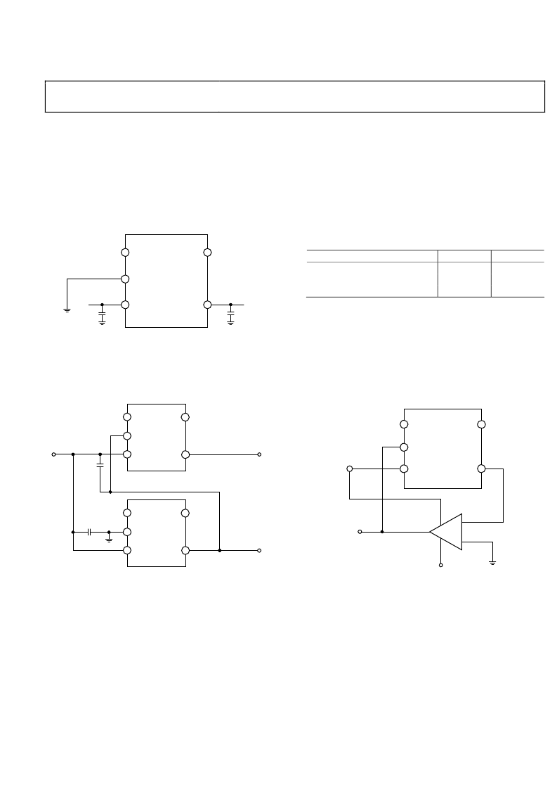
BASIC VOLTAGE REFERENCE CONNECTION
The circuit in Figure 33 illustrates the basic configuration for
the ADR36x family. Decoupling capacitors are not required for
circuit stability. The ADR36x family is capable of driving
capacitive loads from 0 μF to 10 μF. However, a 0.1 μF ceramic
output capacitor is recommended to absorb and deliver the
charge as is required by a dynamic load.
Rev. A | Page 17 of 20
1
2
3
NC
GND
V
IN
ADR36x
5
4
TRIM
V
OUT
INPUT
0.1
μ
F
OUTPUT
0.1
μ
F
0
Figure 33. Basic Configuration for the ADR36x Family
Stacking Reference ICs for Arbitrary Outputs
Some applications can require two reference voltage sources,
which are a combined sum of standard outputs. Figure 34 shows
how this stacked output reference can be implemented.
0
NC
NC
GND
GND
V
IN
V
IN
ADR36x
ADR36x
TRIM
TRIM
V
OUT
V
OUT
1
1
2
2
3
3
5
5
4
4
V
OUT2
V
OUT1
V
IN
C1
0.1
μ
F
C2
0.1
F
Figure 34. Stacking Voltage References with the ADR36x
Two reference ICs are used and fed from an unregulated input,
V
IN
. The outputs of the individual ICs are connected in series,
which provides two output voltages, V
OUT1
and V
OUT2
. V
OUT1
is
the terminal voltage of U1, while V
OUT2
is the sum of this voltage
and the terminal voltage of U2. U1 and U2 are chosen for the
two voltages that supply the required outputs (see Table 10). For
example, if both U1 and U2 are ADR361s, V
OUT1
is 2.5 V and
V
OUT2
is 5.0 V.
Table 10. Output
U1/U2
ADR361/ADR365
ADR361/ADR361
ADR365/ADR361
A Negative Precision Reference Without Precision
Resistors
A negative reference is easily generated by adding an op amp,
A1 and is configured in Figure 35. V
OUTF
and V
OUTS
are at virtual
ground and, therefore, the negative reference can be taken
directly from the output of the op amp. The op amp must be
dual-supply, low offset, and rail-to-rail if the negative supply
voltage is close to the reference output.
V
OUT1
2.5
2.5
5
V
OUT2
7.5
5.0
7.5
0
NC
GND
V
IN
ADR36x
TRIM
V
OUT
1
2
3
–
+
5
4
–V
REF
–V
DD
+V
DD
Figure 35. Negative Reference
相關PDF資料 |
PDF描述 |
|---|---|
| ADR365A | Low Power, Low Noise Voltage References with Sink/Source Capability |
| ADR365AUJZ-REEL7 | Low Power, Low Noise Voltage References with Sink/Source Capability |
| ADR365B | Low Power, Low Noise Voltage References with Sink/Source Capability |
| ADR365BUJZ-REEL7 | Low Power, Low Noise Voltage References with Sink/Source Capability |
| ADR366 | Low Power, Low Noise Voltage References with Sink/Source Capability |
相關代理商/技術參數 |
參數描述 |
|---|---|
| ADR365A | 制造商:AD 制造商全稱:Analog Devices 功能描述:Low Power, Low Noise Voltage References with Sink/Source Capability |
| ADR365AUJZ-R2 | 功能描述:IC VREF SERIES PREC 5V TSOT-23-5 RoHS:是 類別:集成電路 (IC) >> PMIC - 電壓基準 系列:- 標準包裝:1,000 系列:- 基準類型:旁路,可調節,精度 輸出電壓:2.495 V ~ 36 V 容差:±0.5% 溫度系數:標準值 34ppm/°C 輸入電壓:2.495 V ~ 36 V 通道數:1 電流 - 陰極:1mA 電流 - 靜態:- 電流 - 輸出:100mA 工作溫度:0°C ~ 70°C 安裝類型:表面貼裝 封裝/外殼:TO-243AA 供應商設備封裝:SOT-89-3 包裝:帶卷 (TR) |
| ADR365AUJZ-R2 | 制造商:Analog Devices 功能描述:IC, SERIES V-REF, 5V, 8mV, TSOT-5 |
| ADR365AUJZ-REEL7 | 功能描述:IC VREF SERIES PREC 5V TSOT-23-5 RoHS:是 類別:集成電路 (IC) >> PMIC - 電壓基準 系列:- 產品培訓模塊:Voltage Reference Basics 標準包裝:100 系列:- 基準類型:旁路,精度 輸出電壓:4.096V 容差:±0.075% 溫度系數:50ppm/°C 輸入電壓:- 通道數:1 電流 - 陰極:1µA 電流 - 靜態:- 電流 - 輸出:10mA 工作溫度:0°C ~ 70°C 安裝類型:表面貼裝 封裝/外殼:8-SOIC(0.154",3.90mm 寬) 供應商設備封裝:8-SOIC 包裝:管件 |
| ADR365B | 制造商:AD 制造商全稱:Analog Devices 功能描述:Low Power, Low Noise Voltage References with Sink/Source Capability |
發布緊急采購,3分鐘左右您將得到回復。