- 您現在的位置:買賣IC網 > PDF目錄374026 > ADR370 (Analog Devices, Inc.) Precision Low Power 2.048 V SOT-23 Voltage Reference PDF資料下載
參數資料
| 型號: | ADR370 |
| 廠商: | Analog Devices, Inc. |
| 英文描述: | Precision Low Power 2.048 V SOT-23 Voltage Reference |
| 中文描述: | 精密低功耗2.048 V SOT - 23封裝電壓基準 |
| 文件頁數: | 6/12頁 |
| 文件大小: | 182K |
| 代理商: | ADR370 |
REV. A
–6–
ADR370
PARAMETER DEFINITIONS
Temperature Coefficient
Temperature coefficient is the change of output voltage with
respect to operating temperature changes, normalized by the
output voltage at 25
°
C. This parameter is expressed in ppm/
°
C
and can be determined with the following equation
( )
°
(
25
where:
V
O
(
25
°
C)
=
V
O
at 25
°
C.
V
O
(T
1
)
=
V
O
at Temperature 1.
V
O
(T
2
)
=
V
O
at Temperature 2.
Line Regulation
Line regulation is the change in output voltage due to a specified
change in input voltage. This parameter accounts for the effects
of self-heating. Line regulation is expressed in either percent per
volt, parts-per-million per volt, or microvolts per volt change in
input voltage.
Load Regulation
Load regulation is the change in output voltage due to a specified
change in load current. This parameter accounts for the effects
of self-heating. Load regulation is expressed in either microvolts
per milliampere, parts-per-million per milliampere, or ohms of
dc output resistance.
Long Term Stability
Long term stability is the typical shift of output voltage at 25
°
C
on a sample of parts subjected to a test of 1,000 hours at 25
°
C.
V
V
t
V
t
V
t
V
V
t
O
( )
0
where:
V
O
(T
1
)
=
V
O
at 25
°
C at time 0.
V
O
(T
2
)
=
V
O
at 25
°
C after 1,000 hours operation at 25
°
C.
Thermal Hysteresis
Thermal hysteresis is defined as the change of output voltage after
the device is cycled through temperature from +25
°
C to
–
40
°
C
to +125
°
C and back to +25
°
C. This is a typical value from a sample
of parts put through such a cycle.
=
°
(
[
(
25
where:
V
O
(
25
°
C)
=
V
O
at 25
°
C.
V
O_TC
=
V
O
at 25
°
C after temperature cycle at +25
°
C to
–
40
°
C
to +125
°
C and back to +25
°
C.
TCV
ppm
C
°
V
T
V
T
( )
2
V
C
T
(
T
O
O
O
O
=
)
×
)
×
2
1
1
6
10
(1)
V
ppm
t
O
O
O
( )
0
O
O
O
=
( )
]
=
( )
[
( )
1
×
0
6
10
(2)
V
V
C
V
V
ppm
V
C
V
C
°
V
O
HYS
O
O TC
_
°
O
HYS
O
O TC
_
)
O
_
_
)
(
]
=
)
×
25
25
10
6
(3)
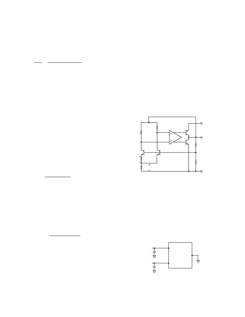
THEORY OF OPERATION
The ADR370 uses the band-gap concept to produce a stable,
low temperature coefficient voltage reference suitable for high
accuracy data acquisition components and systems. This device
makes use of underlying temperature characteristics of a silicon
transistor
’
s base-emitter voltage (V
BE
) in the forward biased
operating region. Under this condition, all such transistors have
a
–
2 mV/
°
C temperature coefficient (TC) and a V
BE
that, when
extrapolated to absolute zero, 0 K, (with collector current pro-
portional to absolute temperature) approximates the silicon
band-gap voltage. By summing a voltage that has an equal and
opposite temperature coefficient of 2 mV/
°
C with a V
BE
of a
forward biased transistor, an almost zero TC reference can be
developed. The simplified circuit diagram in Figure 1 shows how
a compensating voltage, V1, is achieved by driving two transistors
at different current densities and amplifying the resultant V
BE
difference (
V
BE
, which has a positive TC). The sum (V
BG
) of V
BE
and V1 is then buffered and amplified to produce a stable reference
voltage of 2.048 V at the output.
V
IN
V
OUT
GND
V
DS
R5
R6
R4
R3
R2
R1
V1
Figure 1. Simplified Schematic
Applying the ADR370
In order to achieve the specified performance, two external
components should be used in conjunction with the ADR370,
a 4.7
μ
F capacitor and a 1
μ
F capacitor should be applied to the
input and output, respectively. Figure 2 shows the ADR370 with
both the input and output capacitors attached.
For further transient response optimization, an additional 0.1
μ
F
capacitor in parallel with the 4.7
μ
F input capacitor can be used.
A 1
μ
F output capacitor will provide stable performance for all
loading conditions. The ADR370 can, however, operate under
low (
–
100
μ
A < I
OUT
< +100
μ
A) current conditions with just a
0.2
μ
F output capacitor and a 1
μ
F input capacitor.
C
IN
V
IN
ADR370
GND
4.7 F
C
OUT
V
OUT
1 F
Figure 2. Typical Connection Diagram
相關PDF資料 |
PDF描述 |
|---|---|
| ADR370ART-R2 | Precision Low Power 2.048 V SOT-23 Voltage Reference |
| ADR370ART-REEL7 | Precision Low Power 2.048 V SOT-23 Voltage Reference |
| ADR370BRT-R2 | Precision Low Power 2.048 V SOT-23 Voltage Reference |
| ADR370BRT-REEL7 | Precision Low Power 2.048 V SOT-23 Voltage Reference |
| ADR380 | Precision Low-Drift 2.048 V/2.500 V SOT-23 Voltage References |
相關代理商/技術參數 |
參數描述 |
|---|---|
| ADR370ART-R2 | 功能描述:IC VREF SERIES PREC SOT-23-3 RoHS:否 類別:集成電路 (IC) >> PMIC - 電壓基準 系列:- 標準包裝:3,000 系列:- 基準類型:旁路,精度 輸出電壓:5V 容差:±0.5% 溫度系數:100ppm/°C 輸入電壓:- 通道數:1 電流 - 陰極:80µA 電流 - 靜態:- 電流 - 輸出:15mA 工作溫度:-40°C ~ 85°C 安裝類型:表面貼裝 封裝/外殼:TO-236-3,SC-59,SOT-23-3 供應商設備封裝:SOT-23-3 包裝:帶卷 (TR) 其它名稱:LM4040CIM3-5.0MLTRLM4040CIM3-5.0MLTR-ND |
| ADR370ART-REEL7 | 制造商:Analog Devices 功能描述:V-Ref Precision 2.048V 5mA 3-Pin SOT-23 T/R 制造商:Rochester Electronics LLC 功能描述:+4.096V REFERENCE - Tape and Reel |
| ADR370ARTZ-REEL7 | 功能描述:IC VREF SERIES PREC SOT-23-3 RoHS:是 類別:集成電路 (IC) >> PMIC - 電壓基準 系列:- 標準包裝:1 系列:- 基準類型:串聯,精度 輸出電壓:4.5V 容差:±800µV 溫度系數:1ppm/°C 輸入電壓:13.5 V ~ 22 V 通道數:1 電流 - 陰極:- 電流 - 靜態:7mA 電流 - 輸出:10mA 工作溫度:-55°C ~ 125°C 安裝類型:表面貼裝 封裝/外殼:20-LCC 供應商設備封裝:20-CLCC 包裝:管件 |
| ADR370BRT-R2 | 功能描述:IC VREF SERIES PREC SOT-23-3 RoHS:否 類別:集成電路 (IC) >> PMIC - 電壓基準 系列:- 標準包裝:3,000 系列:- 基準類型:旁路,精度 輸出電壓:5V 容差:±0.5% 溫度系數:100ppm/°C 輸入電壓:- 通道數:1 電流 - 陰極:80µA 電流 - 靜態:- 電流 - 輸出:15mA 工作溫度:-40°C ~ 85°C 安裝類型:表面貼裝 封裝/外殼:TO-236-3,SC-59,SOT-23-3 供應商設備封裝:SOT-23-3 包裝:帶卷 (TR) 其它名稱:LM4040CIM3-5.0MLTRLM4040CIM3-5.0MLTR-ND |
| ADR370BRT-REEL7 | 制造商:Rochester Electronics LLC 功能描述:+4.096V REFERENCE - Tape and Reel 制造商:Analog Devices 功能描述: |
發布緊急采購,3分鐘左右您將得到回復。