- 您現(xiàn)在的位置:買賣IC網(wǎng) > PDF目錄374028 > ADR421 (Analog Devices, Inc.) Ultraprecision Low Noise, 2.048 V/2.500 V/ 3.00 V/5.00 V XFET Voltage References PDF資料下載
參數(shù)資料
| 型號: | ADR421 |
| 廠商: | Analog Devices, Inc. |
| 英文描述: | Ultraprecision Low Noise, 2.048 V/2.500 V/ 3.00 V/5.00 V XFET Voltage References |
| 中文描述: | 超精密低噪聲,2.048 V/2.500第V / 3.00 V/5.00 V XFET電壓基準 |
| 文件頁數(shù): | 13/16頁 |
| 文件大小: | 223K |
| 代理商: | ADR421 |
REV. B
ADR420/ADR421/ADR423/ADR425
–13–
Reference for Converters in Optical Network Control Circuits
In the upcoming high-capacity, all-optical router network, Figure 4
employs arrays of micromirrors to direct and route optical
signals from fiber to fiber, without first converting them to
electrical form, which reduces the communication speed. The tiny
micromechanical mirrors are positioned so that each is illuminated
by a single wavelength that carries unique information and can be
passed to any desired input and output fiber. The mirrors are tilted
by the dual-axis actuators controlled by precision ADCs and
DACs within the system. Due to the microscopic movement of
the mirrors, not only is the precision of the converters important,
but the noise associated with these controlling converters is also
extremely critical, because total noise within the system can
be multiplied by the numbers of converters employed. As a result,
the ADR42x is necessary for this application for its exceptional
low noise to maintain the stability of the control loop.
CONTROL
ELECTRONICS
PREAMP
AMPL
AMPL
ADR421
ADR421
ADR421
DAC
DAC
ADC
DSP
MEMS MIRROR
ACTIVATOR
RIGHT
ACTIVATOR
LEFT
GIMBAL + SENSOR
SOURCE FIBER
LASER BEAM
DESTINATION
FIBER
Figure 4. All-Optical Router Network
A Negative Precision Reference without Precision Resistors
In many current-output CMOS DAC applications, where the
output signal voltage must be of the same polarity as the reference
voltage, it is often required to reconfigure a current-switching
DAC into a voltage-switching DAC through the use of a 1.25 V
reference, an op amp, and a pair of resistors. Using a current-
switching DAC directly requires the need for an additional
operational amplifier at the output to reinvert the signal. A
negative voltage reference is then desirable from the point that
an additional operational amplifier is not required for either
reinversion (current-switching mode) or amplification (voltage-
switching mode) of the DAC output voltage. In general, any
positive voltage reference can be converted into a negative voltage
reference through the use of an operational amplifier and a pair of
matched resistors in an inverting configuration. The disadvantage
to that approach is that the largest single source of error in the
circuit is the relative matching of the resistors used.
A negative reference can easily be generated by adding a precision
op amp and configuring as in Figure 5. V
OUT
is at virtual ground
and, therefore, the negative reference can be taken directly from
the output of the op amp. The op amp must be dual supply, low
offset, and have rail-to-rail capability if negative supply voltage
is close to the reference output.
+V
DD
–
V
DD
–
V
REF
V
OUT
V
IN
GND
4
ADR42x
A1 = OP777, OP193
A1
6
2
Figure 5. Negative Reference
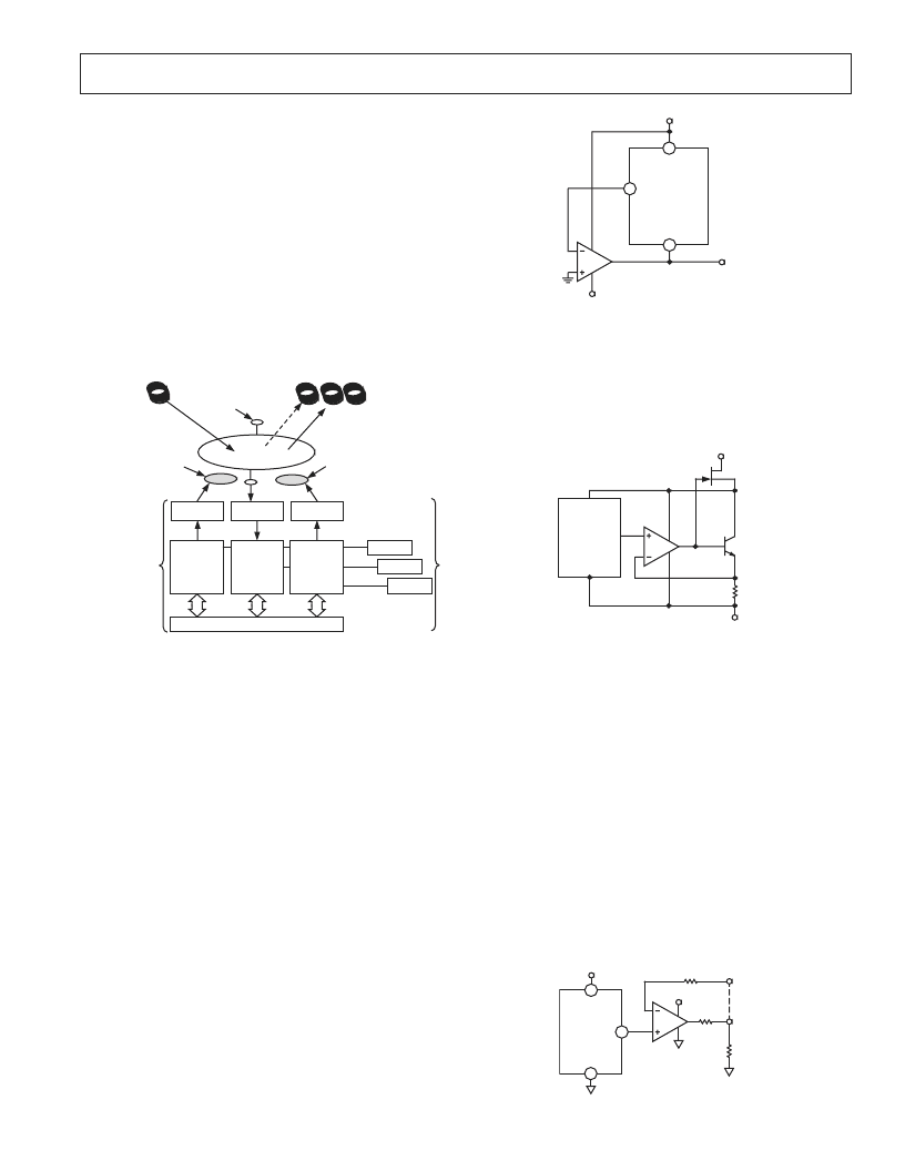
High-Voltage Floating Current Source
The circuit of Figure 6 can be used to generate a floating current
source with minimal self-heating. This particular configuration
can operate on high supply voltages determined by the breakdown
voltage of the N-channel JFET.
V
IN
GND
+V
S
ADR42x
R
L
2.10k
–
V
S
2N3904
V
OUT
SST111
VISHAY
OP90
Figure 6. High-Voltage Floating Current Source
Kelvin Connections
In many portable instrumentation applications, where PC board
cost and area go hand-in-hand, circuit interconnects are very
often of dimensionally minimum width. These narrow lines can
cause large voltage drops if the voltage reference is required to
provide load currents to various functions. In fact, a circuit
’
s
interconnects can exhibit a typical line resistance of 0.45 m
/
square (1 oz. Cu, for example). Force and sense connections,
also referred to as Kelvin connections, offer a convenient method
of eliminating the effects of voltage drops in circuit wires. Load
currents flowing through wiring resistance produce an error
(V
ERROR
= R
×
I
L
) at the load. However, the Kelvin connection
of Figure 7 overcomes the problem by including the wiring
resistance within the forcing loop of the op amp. Since the op
amp senses the load voltage, op amp loop control forces the
output to compensate for the wiring error and to produce the
correct voltage at the load.
V
IN
GND
4
R
LW
ADR42x
V
FORCE
A1
V
IN
V
OUT
R
LW
R
L
V
SENSE
A1 = OP191
2
6
Figure 7. Advantage of Kelvin Connection
相關(guān)PDF資料 |
PDF描述 |
|---|---|
| ADR423 | Ultraprecision Low Noise, 2.048 V/2.500 V/ 3.00 V/5.00 V XFET Voltage References |
| ADR423AR | Ultraprecision Low Noise, 2.048 V/2.500 V/ 3.00 V/5.00 V XFET Voltage References |
| ADR421BR-REEL7 | 10/100-ST SM PLUS |
| ADR439AR | Ultralow Noise XFET Voltage References with Current Sink and Source Capability |
| ADR439AR-REEL7 | Ultralow Noise XFET Voltage References with Current Sink and Source Capability |
相關(guān)代理商/技術(shù)參數(shù) |
參數(shù)描述 |
|---|---|
| ADR4210001RMZ7 | 制造商:Analog Devices 功能描述: |
| ADR421AR | 功能描述:IC VREF SERIES PREC 2.5V 8-SOIC RoHS:否 類別:集成電路 (IC) >> PMIC - 電壓基準 系列:XFET® 標準包裝:3,000 系列:- 基準類型:旁路,精度 輸出電壓:5V 容差:±0.5% 溫度系數(shù):100ppm/°C 輸入電壓:- 通道數(shù):1 電流 - 陰極:80µA 電流 - 靜態(tài):- 電流 - 輸出:15mA 工作溫度:-40°C ~ 85°C 安裝類型:表面貼裝 封裝/外殼:TO-236-3,SC-59,SOT-23-3 供應(yīng)商設(shè)備封裝:SOT-23-3 包裝:帶卷 (TR) 其它名稱:LM4040CIM3-5.0MLTRLM4040CIM3-5.0MLTR-ND |
| ADR421AR | 制造商:Analog Devices 功能描述:SEMICONDUCTORS ((NW)) |
| ADR421ARM | 制造商:Analog Devices 功能描述:V-Ref Precision 2.5V 10mA 8-Pin MSOP Tube 制造商:Analog Devices 功能描述:IC VOLT REF |
| ADR421ARM-REEL7 | 制造商:Rochester Electronics LLC 功能描述: 制造商:Analog Devices 功能描述:IC,VOLT REFERENCE,FIXED,2.5V,TSSOP,8PIN,PLASTIC |
發(fā)布緊急采購,3分鐘左右您將得到回復(fù)。