- 您現(xiàn)在的位置:買賣IC網(wǎng) > PDF目錄374028 > ADR430AR-REEL7 (ANALOG DEVICES INC) Ultralow Noise XFET Voltage References with Current Sink and Source Capability PDF資料下載
參數(shù)資料
| 型號: | ADR430AR-REEL7 |
| 廠商: | ANALOG DEVICES INC |
| 元件分類: | 基準電壓源/電流源 |
| 英文描述: | Ultralow Noise XFET Voltage References with Current Sink and Source Capability |
| 中文描述: | 1-OUTPUT THREE TERM VOLTAGE REFERENCE, 2.048 V, PDSO8 |
| 封裝: | MS-012AA, SOIC-8 |
| 文件頁數(shù): | 15/24頁 |
| 文件大小: | 868K |
| 代理商: | ADR430AR-REEL7 |
ADR430/ADR431/ADR433/ADR434/ADR435/ADR439
THEORY OF OPERATION
The ADR43x series of references uses a new reference generation
technique known as XFET (eXtra implanted junction FET).
This technique yields a reference with low supply current, good
thermal hysteresis, and exceptionally low noise. The core of the
XFET reference consists of two junction field-effect transistors
(JFETs), one of which has an extra channel implant to raise its
pinch-off voltage. By running the two JFETs at the same drain
current, the difference in pinch-off voltage can be amplified and
used to form a highly stable voltage reference.
Rev. B | Page 15 of 24
The intrinsic reference voltage is around 0.5 V with a negative
temperature coefficient of about –120 ppm/°C. This slope is
essentially constant to the dielectric constant of silicon and can
be closely compensated by adding a correction term generated
in the same fashion as the proportional-to-temperature (PTAT)
term used to compensate band gap references. The big advantage
of an XFET reference is that the correction term is some 30 times
lower (therefore, requiring less correction) than for a band gap
reference, resulting in much lower noise, because most of the
noise of a band gap reference comes from the temperature
compensation circuitry.
Figure 29 shows the basic topology of the ADR43x series. The
temperature correction term is provided by a current source
with a value designed to be proportional to absolute temperature.
The general equation is
(
PTAT
P
OUT
I
R1
V
Δ
G
V
)
×
×
=
(1)
where:
G
is the gain of the reciprocal of the divider ratio.
V
P
is the difference in pinch-off voltage between the two JFETs.
I
PTAT
is the positive temperature coefficient correction current.
ADR43x devices are created by on-chip adjustment of R2 and
R3 to achieve 2.048 V or 2.500 V, respectively, at the reference
output.
*
I
PTAT
I
1
I
1
*EXTRA CHANNEL IMPLANT
V
OUT
= G(
V
P
– R1
×
I
PTAT
)
R2
V
IN
V
OUT
GND
R3
R1
V
P
0
ADR43x
Figure 29. Simplified Schematic Device
Power Dissipation Considerations
The ADR43x family of references is guaranteed to deliver load
currents to 10 mA with an input voltage that ranges from 4.5 V
to 18 V. When these devices are used in applications at higher
currents, users should use the following equation to account for
the temperature effects due to the power dissipation increases.
A
JA
D
J
T
P
T
+
θ
×
=
(2)
where:
T
J
and
T
A
are the junction and ambient temperatures,
respectively.
P
D
is the device power dissipation.
θ
JA
is the device package thermal resistance.
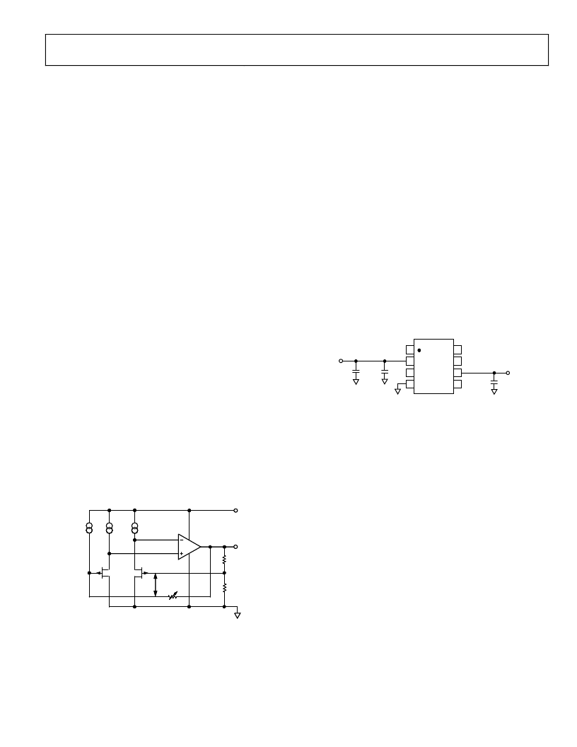
BASIC VOLTAGE REFERENCE CONNECTIONS
Voltage references, in general, require a bypass capacitor
connected from V
OUT
to GND. The circuit in Figure 30
illustrates the basic configuration for the ADR43x family of
references. Other than a 0.1 μF capacitor at the output to help
improve noise suppression, a large output capacitor at the
output is not required for circuit stability.
+
NIC = NO INTERNAL CONNECTION
TP = TEST PIN (DO NOT CONNECT)
1
2
3
4
5
8
6
7
ADR43x
TOP VIEW
(Not to Scale)
TP
NIC
OUTPUT
TRIM
TP
NIC
V
IN
10
μ
F
0.1
μ
F
0.1
μ
F
0
Figure 30. Basic Voltage Reference Configuration
NOISE PERFORMANCE
The noise generated by the ADR43x family of references is
typically less than 3.75 μV p-p over the 0.1 Hz to 10.0 Hz band
for ADR430, ADR431, and ADR433. Figure 22 shows the 0.1
Hz to 10 Hz noise of the ADR431, which is only 3.5 μV p-p. The
noise measurement is made with a band-pass filter made of a
2-pole high-pass filter with a corner frequency at 0.1 Hz and a
2-pole low-pass filter with a corner frequency at 10.0 Hz.
TURN-ON TIME
Upon application of power (cold start), the time required for
the output voltage to reach its final value within a specified
error band is defined as the turn-on settling time. Two compo-
nents normally associated with this are the time for the active
circuits to settle and the time for the thermal gradients on the
chip to stabilize. Figure 17 and Figure 18 show the turn-on
settling time for the ADR431.
相關(guān)PDF資料 |
PDF描述 |
|---|---|
| ADR430ARM | Ultralow Noise XFET Voltage References with Current Sink and Source Capability |
| ADR430ARM-REEL7 | Ultralow Noise XFET Voltage References with Current Sink and Source Capability |
| ADR434A | Ultralow Noise XFET Voltage References with Current Sink and Source Capability |
| ADR434AR | Ultralow Noise XFET Voltage References with Current Sink and Source Capability |
| ADR434ARM | Ultralow Noise XFET Voltage References with Current Sink and Source Capability |
相關(guān)代理商/技術(shù)參數(shù) |
參數(shù)描述 |
|---|---|
| ADR430ARZ | 功能描述:IC VREF SERIES PREC 2.048V 8SOIC RoHS:是 類別:集成電路 (IC) >> PMIC - 電壓基準 系列:XFET® 標準包裝:1,000 系列:- 基準類型:旁路,可調(diào)節(jié),精度 輸出電壓:2.495 V ~ 36 V 容差:±0.5% 溫度系數(shù):標準值 34ppm/°C 輸入電壓:2.495 V ~ 36 V 通道數(shù):1 電流 - 陰極:1mA 電流 - 靜態(tài):- 電流 - 輸出:100mA 工作溫度:0°C ~ 70°C 安裝類型:表面貼裝 封裝/外殼:TO-243AA 供應(yīng)商設(shè)備封裝:SOT-89-3 包裝:帶卷 (TR) |
| ADR430ARZ-REEL7 | 功能描述:IC VREF SERIES PREC 2.048V 8SOIC RoHS:是 類別:集成電路 (IC) >> PMIC - 電壓基準 系列:XFET® 標準包裝:2,000 系列:- 基準類型:旁路,可調(diào)節(jié),精度 輸出電壓:1.24 V ~ 16 V 容差:±0.5% 溫度系數(shù):- 輸入電壓:1.24 V ~ 16 V 通道數(shù):1 電流 - 陰極:100µA 電流 - 靜態(tài):- 電流 - 輸出:20mA 工作溫度:-40°C ~ 85°C 安裝類型:通孔 封裝/外殼:TO-226-3、TO-92-3(TO-226AA)成形引線 供應(yīng)商設(shè)備封裝:TO-92-3 包裝:帶卷 (TR) |
| ADR430B | 制造商:AD 制造商全稱:Analog Devices 功能描述:Ultralow Noise XFET Voltage References with Current Sink and Source Capability |
| ADR430BR | 制造商:Rochester Electronics LLC 功能描述: 制造商:Analog Devices 功能描述: |
| ADR430BR-REEL7 | 制造商:Analog Devices 功能描述:V-Ref Precision 2.048V 30mA 8-Pin SOIC N T/R |
發(fā)布緊急采購,3分鐘左右您將得到回復(fù)。