- 您現在的位置:買賣IC網 > PDF目錄374028 > ADR439BR (ANALOG DEVICES INC) Ultralow Noise XFET Voltage References with Current Sink and Source Capability PDF資料下載
參數資料
| 型號: | ADR439BR |
| 廠商: | ANALOG DEVICES INC |
| 元件分類: | 基準電壓源/電流源 |
| 英文描述: | Ultralow Noise XFET Voltage References with Current Sink and Source Capability |
| 中文描述: | 1-OUTPUT THREE TERM VOLTAGE REFERENCE, 4.5 V, PDSO8 |
| 封裝: | MS-012AA, SOIC-8 |
| 文件頁數: | 17/24頁 |
| 文件大小: | 868K |
| 代理商: | ADR439BR |
ADR430/ADR431/ADR433/ADR434/ADR435/ADR439
Rev. B | Page 17 of 24
+V
DD
–
V
REF
GND
4
V
IN
V
OUT
ADR43x
A1
–
V
DD
A1 = OP777, OP193
2
6
0
Figure 33. Negative Reference
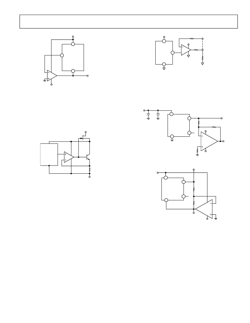
HIGH VOLTAGE FLOATING CURRENT SOURCE
The circuit in Figure 34 can be used to generate a floating
current source with minimal self-heating. This particular
configuration can operate on high supply voltages determined
by the breakdown voltage of the N-channel JFET.
V
IN
V
OUT
GND
OP90
+V
S
SST111
VISHAY
2N3904
R
2.1k
–V
S
ADR43x
0
Figure 34. High Voltage Floating Current Source
KELVIN CONNECTIONS
In many portable instrumentation applications where PC board
cost and area go hand-in-hand, circuit interconnects are very
often of dimensionally minimum width. These narrow lines can
cause large voltage drops if the voltage reference is required to
provide load currents to various functions. In fact, a circuit’s
interconnects can exhibit a typical line resistance of 0.45 m/
square (1 oz. Cu, for example). Force and sense connections,
also referred to as Kelvin connections, offer a convenient
method of eliminating the effects of voltage drops in circuit
wires. Load currents flowing through wiring resistance produce
an error (V
ERROR
= R × I
L
) at the load. However, the Kelvin
connection of Figure 35 overcomes the problem by including
the wiring resistance within the forcing loop of the op amp.
Because the op amp senses the load voltage, the op amp loop
control forces the output to compensate for the wiring error and
to produce the correct voltage at the load.
V
IN
V
OUT
GND
4
R
LW
R
L
V
SENSE
V
FORCE
R
LW
V
IN
2
6
ADR43x
A1 = OP191
A1
0
+
Figure 35. Advantage of Kelvin Connection
DUAL POLARITY REFERENCES
Dual polarity references can easily be made with an op amp and
a pair of resistors. In order not to defeat the accuracy obtained
by ADR43x, it is imperative to match the resistance tolerance as
well as the temperature coefficient of all the components.
6
2
V
IN
4
5
–
10V
V
IN
V
OUT
GND
TRIM
R1
R2
10k
V–
R3
5k
V+
+10V
–5V
+5V
1
μ
F
0.1
μ
F
U1
ADR435
OP1177
10k
0
Figure 36. +5 V and 5 V References Using ADR435
6
2
4
5
V
IN
V
OUT
GND
TRIM
R1
5.6k
U2
V–
V+
+10V
U1
ADR435
OP1177
+2.5V
–2.5V
R2
5.6k
0
–10V
Figure 37. +2.5 V and 2.5 V References Using ADR435
相關PDF資料 |
PDF描述 |
|---|---|
| ADR434ARM-REEL7 | Ultralow Noise XFET Voltage References with Current Sink and Source Capability |
| ADR434B | Ultralow Noise XFET Voltage References with Current Sink and Source Capability |
| ADR434BR | Ultralow Noise XFET Voltage References with Current Sink and Source Capability |
| ADR434BR-REEL7 | Ultralow Noise XFET Voltage References with Current Sink and Source Capability |
| ADR435 | Ultralow Noise XFET Voltage References with Current Sink and Source Capability |
相關代理商/技術參數 |
參數描述 |
|---|---|
| ADR439BR-REEL7 | 制造商:Analog Devices 功能描述:V-Ref Precision 4.5V 30mA 8-Pin SOIC N T/R |
| ADR439BRZ | 制造商:Analog Devices 功能描述:V-Ref Precision 4.5V 30mA 8-Pin SOIC N Tube |
| ADR439BRZ-REEL7 | 功能描述:IC VREF SERIES PREC 4.5V 8-SOIC RoHS:是 類別:集成電路 (IC) >> PMIC - 電壓基準 系列:XFET® 產品培訓模塊:Lead (SnPb) Finish for COTS Obsolescence Mitigation Program 標準包裝:50 系列:- 基準類型:串聯,隱埋式齊納 輸出電壓:2.5V 容差:±0.04% 溫度系數:2ppm/°C 輸入電壓:8 V ~ 36 V 通道數:1 電流 - 陰極:- 電流 - 靜態:3mA 電流 - 輸出:15mA 工作溫度:0°C ~ 70°C 安裝類型:通孔 封裝/外殼:8-DIP(0.300",7.62mm) 供應商設備封裝:8-PDIP 包裝:管件 |
| ADR440 | 制造商:AD 制造商全稱:Analog Devices 功能描述:Ultralow Noise, LDO XFET Voltage References with Current Sink and Source |
| ADR440_10 | 制造商:AD 制造商全稱:Analog Devices 功能描述:Ultralow Noise, LDO XFET Voltage References with Current Sink and Source |
發布緊急采購,3分鐘左右您將得到回復。