- 您現(xiàn)在的位置:買(mǎi)賣IC網(wǎng) > PDF目錄379646 > ADS-943GC (Electronic Theatre Controls, Inc.) 14-Bit, 3MHz, Low-Distortion Sampling A/D Converters PDF資料下載
參數(shù)資料
| 型號(hào): | ADS-943GC |
| 廠商: | Electronic Theatre Controls, Inc. |
| 元件分類: | 串行ADC |
| 英文描述: | 14-Bit, 3MHz, Low-Distortion Sampling A/D Converters |
| 中文描述: | 14位,3MHz的,低失真的采樣A / D轉(zhuǎn)換器 |
| 文件頁(yè)數(shù): | 4/8頁(yè) |
| 文件大小: | 166K |
| 代理商: | ADS-943GC |
ADS -943
4
CALIBRATION PROCEDURE
Any offset and/or gain calibration procedures should not be
implemented until devices are fully warmed up. To avoid
interaction, offset must be adjusted before gain. The ranges of
adjustment for the circuits in Figures 2 and 3 are guaranteed to
compensate for the ADS-943's initial accuracy errors and may
not be able to compensate for additional system errors.
A/D converters are calibrated by positioning their digital outputs
exactly on the transition point between two adjacent digital
output codes. This can be accomplished by connecting LED's
to the digital outputs and adjusting until certain LED's "flicker"
equally between on and off. Other approaches employ digital
comparators or microcontrollers to detect when the outputs
change from one code to the next.
Offset adjusting for the ADS-943 is normally accomplished at
the point where the MSB is a 1 and all other output bits are 0's
and the LSB just changes from a 0 to a 1. This digital output
transition ideally occurs when the applied analog input is
+ LSB (+122μV).
Gain adjusting is accomplished when all bits are 1's and the
LSB just changes from a 1 to a 0. This transition ideally occurs
when the analog input is at +full scale minus 1 LSB's
(+1.99963V).
Zero/Offset Adjust Procedure
1. Apply a train of pulses to the START CONVERT input
(pin 18) so the converter is continuously converting.
2. Apply +122μV to the ANALOG INPUT (pin 21).
3. Adjust the offset potentiometer until the output bits are
10 0000 0000 0000 and the LSB flickers between 0 and 1.
Gain Adjust Procedure
1. Apply +1.99963V to the ANALOG INPUT (pin 21).
2. Adjust the gain potentiometer until all output bits are 1's and
the LSB flickers between 1 and 0.
3. To confirm proper operation of the device, vary the input
signal to obtain the output coding listed in Table 2.
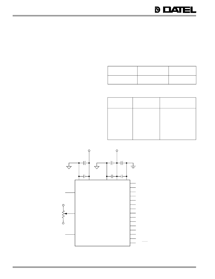
Figure 3. Connection Diagram
0.1μF
0.1μF
4.7μF
+
4.7μF
+
22, 13
24
20
19
ADS-943
–5V
20k
0.1μF
4.7μF
+5V
14
–5V
+5V
21
23
18
1
2
3
4
5
6
7
8
9
10
11
12
15
16
17
BIT 1 (MSB)
BIT 2
BIT 3
BIT 4
BIT 5
BIT 6
BIT 7
BIT 8
BIT 9
BIT 10
BIT 11
BIT 12
BIT 13
BIT 14 (LSB)
EOC
ANALOG
INPUT
START
CONVERT
A single +5V supply should be used for both the +5V analog and +5V digital.
If separate supplies are used, the difference between the two cannot exceed 100mV.
+
ZERO/
OFFSET
ADJUST
INPUT VOLTAGE
RANGE
ZERO ADJUST
+1/2 LSB
GAIN ADJUST
+FS –1 LSB
±2V
+122μV
+1.99963V
Table 1. Gain and Zero Adjust
BIPOLAR
SCALE
INPUT VOLTAGE
(±2V RANGE)
OFFSET BINARY
MSB
LSB
+FS – 1 LSB
+3/4FS
+1/2FS
0
–1/2 FS
–3/4 FS
–FS +1 LSB
–FS
+1.99976
+1.50000
+1.00000
0.00000
–1.00000
–1.50000
1.99976
–2.00000
11 1111 1111 1111
11 1000 0000 0000
11 0000 0000 0000
10 0000 0000 0000
01 0000 0000 0000
00 1000 0000 0000
00 0000 0000 0001
00 0000 0000 0000
Table 2. Output Coding for Bipolar Operation
相關(guān)PDF資料 |
PDF描述 |
|---|---|
| ADS-951 | 18-Bit, 1MHz, Low-Power Sampling A/D Converters |
| ADS-951MC | 18-Bit, 1MHz, Low-Power Sampling A/D Converters |
| ADS-951ME | 18-Bit, 1MHz, Low-Power Sampling A/D Converters |
| ADS-953 | 18-Bit, 1MHz, Low-Distortion Sampling A/D Converters |
| ADS-953MC | 18-Bit, 1MHz, Low-Distortion Sampling A/D Converters |
相關(guān)代理商/技術(shù)參數(shù) |
參數(shù)描述 |
|---|---|
| ADS-943GM | 制造商:Murata Power Solutions 功能描述:ADC Single 2-Step Flash 3Msps 14-bit Parallel 24-Pin SMT |
| ADS-943MC | 制造商:Murata Power Solutions 功能描述:ADC Single 2-Step Flash 3Msps 14-bit Parallel 24-Pin CDDIP |
| ADS-943MM | 制造商:Murata Power Solutions 功能描述:ADC Single 2-Step Flash 3Msps 14-bit Parallel 24-Pin CDDIP |
| ADS944 | 制造商:未知廠家 制造商全稱:未知廠家 功能描述:14-Bit, 5MHz Sampling A/D Converters |
| ADS-944 | 制造商:未知廠家 制造商全稱:未知廠家 功能描述:14-Bit 5MHZ Sampling A/D Converters |
發(fā)布緊急采購(gòu),3分鐘左右您將得到回復(fù)。