- 您現在的位置:買賣IC網 > PDF目錄379646 > ADS-B932 (Electronic Theatre Controls, Inc.) 16-Bit, 2MHz Sampling A/D Converters PDF資料下載
參數資料
| 型號: | ADS-B932 |
| 廠商: | Electronic Theatre Controls, Inc. |
| 元件分類: | 串行ADC |
| 英文描述: | 16-Bit, 2MHz Sampling A/D Converters |
| 中文描述: | 16位,2MHz的采樣A / D轉換器 |
| 文件頁數: | 5/10頁 |
| 文件大小: | 174K |
| 代理商: | ADS-B932 |
ADS-932
5
12) so that the converter is continuously converting.
2. For unipolar or bipolar zero/offset adjust, apply –42μV to the
ANALOG INPUT (pin 3).
3. For bipolar inputs, adjust the offset potentiometer until the
code flickers between 1000 0000 0000 0000 and 0111 1111
1111 1111 with pin 35 tied high (complementary offset
binary) or between 0111 1111 1111 1111 and 1000 0000
0000 0000 with pin 35 tied low (offset binary).
For unipolar inputs, adjust the offset potentiometers until all
output bits are 0's and the LSB flickers between 0 and 1 with
Pin 35 tied high (straight binary) or until all bits are 1's and
the LSB flickers between 0 and 1 with pin 35 tied low
(complementary binary).
4. Two's complement coding requires using BIT 1 (MSB) (pin
29). With pin 35 tied low, adjust the trimpot until the output
code flickers between all 0’s and all 1’s.
Gain Adjust Procedure
1. Apply +2.749874V to the ANALOG INPUT (pin 3).
2. For bipolar inputs adjust the gain potentiometer until all
output bits are 0’s and the LSB flickers between a 1 and 0
with pin 35 tied high (complementary offset binary) or until
all output bits are 1’s and the LSB flickers between a 1 and
0 with pin 35 tied low (offset binary).
3. Two's complement coding requires using BIT 1 (MSB)
(pin 29). With pin 35 tied low, adjust the gain trimpot until
the output code flickers equally between 0111 1111 1111
1111 and 0111 1111 1111 1110.
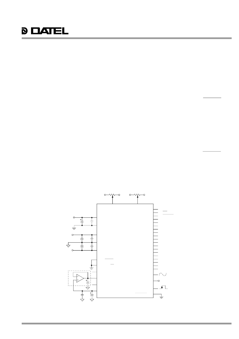
CALIBRATION PROCEDURE
Connect the converter per Figure 2. Any offset/gain
calibration procedures should not be implemented until the
device is fully warmed up. To avoid interaction, adjust offset
before gain. The ranges of adjustment for the circuits in
Figure 2 are guaranteed to compensate for the ADS-932’s
initial accuracy errors and may not be able to compensate for
additional system errors.
A/D converters are calibrated by positioning their digital
outputs exactly on the transition point between two adjacent
digital output codes. This is accomplished by connecting
LED's to the digital outputs and performing adjustments until
certain LED's "flicker" equally between on and off. Other
approaches employ digital comparators or microcontrollers to
detect when the outputs change from one code to the next.
For the ADS-932, offset adjusting is normally accomplished
when the analog input is 0 minus LSB (–42μV). See Table
2b for the proper bipolar output coding.
Gain adjusting is accomplished when the analog input is at
nominal full scale minus 1 LSB's (+2.749874V).
Note: Connect pin 5 to ANALOG GROUND (pin 4) for
operation without zero/offset adjustment. Connect pin 6 to pin
4 for operation without gain adjustment.
Zero/Offset Adjust Procedure
1. Apply a train of pulses to the START CONVERT input (pin
Figure 2. Bipolar Connection Diagram
ADS-932
20k
33
32
29
28
27
26
25
24
23
22
21
20
19
18
17
16
15
14
13
OVERFLOW
EOC
BIT 1 (MSB)
BIT 1 (MSB)
BIT2
BIT 3
BIT 4
BIT 5
BIT 6
BIT 7
BIT 8
BIT 9
BIT 10
BIT 11
BIT 12
BIT 13
BIT 14
BIT 15
BIT 16 (LSB)
ANALOG
DIGITAL
0.1μF
4.7μF
0.1μF
COMP. BITS
4.7μF
+3.2V
REF. OUT
FIFO READ
31
7, 30
35
1
9
+5V
DIGITAL
–5V
+5V
ADJUST
AGAIN
5
6
3
0.1μF
4.7μF
4, 36
37
0.1μF
4.7μF
38
+
+
20k
–5V
+5V
–5V
+5V ANALOG
12
START CONVERT
ANALOG INPUT
34
ENABLE
8
FIFO/DIR
10
FSTAT1
11
FSTAT2
+5V
+5V
+5V
–5V
UNIPOLAR
CONNECT for UNIPOLAR MODE
2
6.8μF
相關PDF資料 |
PDF描述 |
|---|---|
| ADS119 | ECONOLINE: REC3-S_DRW(Z)/H* - 3W DIP Package- 1kVDC Isolation- Wide Input 2:1 & 4:1- Regulated Output- 100% Burned In- UL94V-0 Package Material- Continuous Short Circiut Protection- Efficiency to 80% |
| ADC-B119 | 12-Bit, 10MHz, Low-Power Sampling A/D Converters |
| ADS-119 | LJT 12C 8#20 4#16 SKT RECP |
| ADS-119GC | Circular Connector; No. of Contacts:4; Series:LJT07R; Body Material:Aluminum; Connecting Termination:Crimp; Connector Shell Size:21; Circular Contact Gender:Socket; Circular Shell Style:Jam Nut Receptacle; Insert Arrangement:21-75 |
| ADS-119GM | 12-Bit, 10MHz, Low-Power Sampling A/D Converters |
相關代理商/技術參數 |
參數描述 |
|---|---|
| ADS-B933 | 功能描述:數據轉換 IC 開發(fā)工具 Evaluation Board RoHS:否 制造商:Texas Instruments 產品:Demonstration Kits 類型:ADC 工具用于評估:ADS130E08 接口類型:SPI 工作電源電壓:- 6 V to + 6 V |
| ADS-B935 | 制造商:Murata Power Solutions 功能描述:Evaluation Board |
| ADS-B937 | 功能描述:數據轉換 IC 開發(fā)工具 Evaluation Board RoHS:否 制造商:Texas Instruments 產品:Demonstration Kits 類型:ADC 工具用于評估:ADS130E08 接口類型:SPI 工作電源電壓:- 6 V to + 6 V |
| ADS-B943 | 功能描述:數據轉換 IC 開發(fā)工具 Evaluation Board RoHS:否 制造商:Texas Instruments 產品:Demonstration Kits 類型:ADC 工具用于評估:ADS130E08 接口類型:SPI 工作電源電壓:- 6 V to + 6 V |
| ADS-B944 | 功能描述:數據轉換 IC 開發(fā)工具 Evaluation Board RoHS:否 制造商:Texas Instruments 產品:Demonstration Kits 類型:ADC 工具用于評估:ADS130E08 接口類型:SPI 工作電源電壓:- 6 V to + 6 V |
發(fā)布緊急采購,3分鐘左右您將得到回復。