- 您現在的位置:買賣IC網 > PDF目錄374032 > ADSP-2104 (Analog Devices, Inc.) low cost DSP microcomputers PDF資料下載
參數資料
| 型號: | ADSP-2104 |
| 廠商: | Analog Devices, Inc. |
| 元件分類: | 數字信號處理 |
| 英文描述: | low cost DSP microcomputers |
| 中文描述: | 低成本DSP單片機 |
| 文件頁數: | 6/36頁 |
| 文件大小: | 333K |
| 代理商: | ADSP-2104 |
第1頁第2頁第3頁第4頁第5頁當前第6頁第7頁第8頁第9頁第10頁第11頁第12頁第13頁第14頁第15頁第16頁第17頁第18頁第19頁第20頁第21頁第22頁第23頁第24頁第25頁第26頁第27頁第28頁第29頁第30頁第31頁第32頁第33頁第34頁第35頁第36頁
ADSP-2104/ADSP-2109
–6–
REV. 0
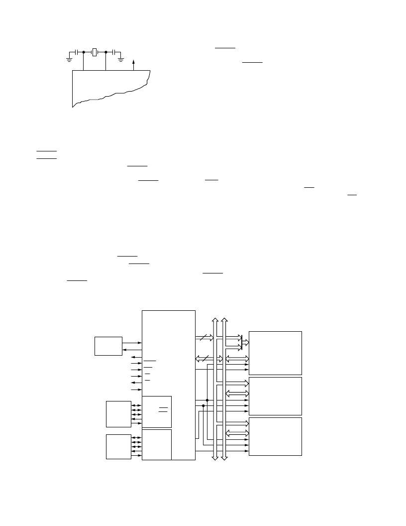
CLKIN
CLKOUT
XTAL
ADSP-2104/
ADSP-2109
Figure 2. External Crystal Connections
A clock output signal (CLK OUT ) is generated by the processor,
synchronized to the processor’s internal cycles.
Reset
The RESET
signal initiates a complete reset of the processor.
T he
RESET
signal must be asserted when the chip is powered
up to assure proper initialization. If the
RESET
signal is applied
during initial power-up, it must be held long enough to allow
the processor’s internal clock to stabilize. If
RESET
is activated
at any time after power-up and the input clock frequency does
not change, the processor’s internal clock continues and does
not require this stabilization time.
T he power-up sequence is defined as the total time required for
the crystal oscillator circuit to stabilize after a valid V
DD
is
applied to the processor and for the internal phase-locked loop
(PLL) to lock onto the specific crystal frequency. A minimum of
2000 t
CK
cycles will ensure that the PLL has locked (this does
not, however, include the crystal oscillator start-up time).
During this power-up sequence the
RESET
signal should be
held low. On any subsequent resets, the
RESET
signal must
meet the minimum pulse width specification, t
RSP
.
T o generate the
RESET
signal, use either an RC circuit with an
external Schmidt trigger or a commercially available reset IC.
(Do not use only an RC circuit.)
T he
RESET
input resets all internal stack pointers to the empty
stack condition, masks all interrupts, and clears the MST AT
register. When
RESET
is released, the boot loading sequence is
performed (provided there is no pending bus request and the
chip is configured for booting, with MMAP = 0). T he first
instruction is then fetched from internal program memory
location 0x0000.
Program Memory Interface
T he on-chip program memory address bus (PMA) and on-chip
program memory data bus (PMD) are multiplexed with the on-
chip data memory buses (DMA, DMD), creating a single
external data bus and a single external address bus. T he external
data bus is bidirectional and is 24 bits wide to allow instruction
fetches from external program memory. Program memory may
contain code and data.
T he external address bus is 14 bits wide.
T he data lines are bidirectional. T he program memory select
(
PMS
) signal indicates accesses to program memory and can be
used as a chip select signal. T he write (
WR
) signal indicates a
write operation and is used as a write strobe. T he read (
RD
)
signal indicates a read operation and is used as a read strobe or
output enable signal.
T he processor writes data from the 16-bit registers to 24-bit
program memory using the PX register to provide the lower
eight bits. When the processor reads 16-bit data from 24-bit
program memory to a 16-bit data register, the lower eight bits
are placed in the PX register.
T he program memory interface can generate 0 to 7 wait states
for external memory devices; default is to 7 wait states after
RESET
.
Figure 3. ADSP-2104/ADSP-2109 System
BR
BG
CLKIN
RESET
IRQ2
BMS
ADSP-2104
or
ADSP-2109
CLKOUT
ADDR
DATA
OE
WE
CS
(OPTIONAL)
1x CLOCK
or
CRYSTAL
PMS
DMS
RD
WR
ADDR
13-0
DATA
23-0
ADDR
DATA
OE
WE
CS
(OPTIONAL)
ADDR
DATA
OE
CS
BOOT
MEMORY
e.g. EPROM
2764
27128
27256
27512
PROGRAM
MEMORY
DATA
MEMORY
&
PERIPHERALS
14
24
D23-22
A13-0
D
15-8
D
23-0
D
23-8
A
13-0
A
13-0
XTAL
MMAP
SERIAL
DEVICE
(OPTIONAL)
SCLK1
RFS1 orIRQ0
TFS1 orIRQ1
DT1 or FO
DR1 or FI
SCLK0
RFS0
TFS0
DT0
DR0
SPORT 1
SPORT 0
SERIAL
DEVICE
(OPTIONAL)
THE TWO MSBs OF THE DATA BUS (D
) ARE USED TO SUPPLY THE TWO MSBs OF THE
BOOT MEMORY EPROM ADDRESS. THIS IS ONLY REQUIRED FOR THE 27256 AND 27512.
相關PDF資料 |
PDF描述 |
|---|---|
| ADSP-2109 | Cap-Free, NMOS, 150mA Low Dropout Regulator with Reverse Current Protection |
| ADSP2104 | Low Cost DSP Microcomputers |
| ADSP-2104KP-80 | Low Cost DSP Microcomputers |
| ADSP-2104LKP-55 | Low Cost DSP Microcomputers |
| ADSP-21160M | DSP Microcomputer |
相關代理商/技術參數 |
參數描述 |
|---|---|
| ADSP-2104BP-80 | 制造商:Analog Devices 功能描述:DSP Fixed-Point 16-Bit 20MHz 20MIPS 68-Pin PLCC 制造商:Analog Devices 功能描述:IC MICROCOMPUTER 16-BIT |
| ADSP-2104BPZ-80 | 功能描述:IC DSP CONTROLLER 16BIT 68PLCC RoHS:是 類別:集成電路 (IC) >> 嵌入式 - DSP(數字式信號處理器) 系列:ADSP-21xx 標準包裝:2 系列:StarCore 類型:SC140 內核 接口:DSI,以太網,RS-232 時鐘速率:400MHz 非易失內存:外部 芯片上RAM:1.436MB 電壓 - 輸入/輸出:3.30V 電壓 - 核心:1.20V 工作溫度:-40°C ~ 105°C 安裝類型:表面貼裝 封裝/外殼:431-BFBGA,FCBGA 供應商設備封裝:431-FCPBGA(20x20) 包裝:托盤 |
| ADSP-2104KP-80 | 制造商:Analog Devices 功能描述:DSP Fixed-Point 16-Bit 20MHz 20MIPS 68-Pin PLCC 制造商:Rochester Electronics LLC 功能描述:- Bulk 制造商:Analog Devices 功能描述:Low cost DSP microcomputer 1 timer 4.5 |
| ADSP-2104L | 制造商:未知廠家 制造商全稱:未知廠家 功能描述:ADSP-2104/ADSP-2104L: Low Cost DSP Microcomputers Data Sheet (Rev. 0. 7/96) |
| ADSP-2104LKP-55 | 制造商:Rochester Electronics LLC 功能描述:- Bulk 制造商:Analog Devices 功能描述: |
發布緊急采購,3分鐘左右您將得到回復。