- 您現在的位置:買賣IC網 > PDF目錄374032 > ADSP-21061KS-160 (ANALOG DEVICES INC) ADSP-2106x SHARC DSP Microcomputer Family PDF資料下載
參數資料
| 型號: | ADSP-21061KS-160 |
| 廠商: | ANALOG DEVICES INC |
| 元件分類: | 數字信號處理 |
| 英文描述: | ADSP-2106x SHARC DSP Microcomputer Family |
| 中文描述: | 48-BIT, 40 MHz, OTHER DSP, PQFP240 |
| 封裝: | MQFP-240 |
| 文件頁數: | 38/47頁 |
| 文件大小: | 367K |
| 代理商: | ADSP-21061KS-160 |
第1頁第2頁第3頁第4頁第5頁第6頁第7頁第8頁第9頁第10頁第11頁第12頁第13頁第14頁第15頁第16頁第17頁第18頁第19頁第20頁第21頁第22頁第23頁第24頁第25頁第26頁第27頁第28頁第29頁第30頁第31頁第32頁第33頁第34頁第35頁第36頁第37頁當前第38頁第39頁第40頁第41頁第42頁第43頁第44頁第45頁第46頁第47頁
–38–
ADSP-21061/ADSP-21061L
REV. B
OUTPUT DRIVE CURRENTS
Figure 27 shows typical I-V characteristics for the output drivers
of the ADSP-2106x. The curves represent the current drive
capability of the output drivers as a function of output voltage.
POWER DISSIPATION
Total power dissipation has two components, one due to inter-
nal circuitry and one due to the switching of external output
drivers. Internal power dissipation is dependent on the instruc-
tion execution sequence and the data operands involved. Inter-
nal power dissipation is calculated in the following way:
P
INT
= I
DDIN
×
V
DD
The external component of total power dissipation is caused by
the switching of output pins. Its magnitude depends on:
– the number of output pins that switch during each cycle (O)
– the maximum frequency at which they can switch (f)
– their load capacitance (C)
– their voltage swing (V
DD
)
and is calculated by:
P
EXT
= O
×
C
×
V
DD
2
×
f
The load capacitance should include the processor’s package
capacitance (C
IN
). The switching frequency includes driving the
load high and then back low. Address and data pins can drive
high and low at a maximum rate of 1/(2t
CK
). The write strobe
can switch every cycle at a frequency of 1/t
CK
. Select pins switch
at 1/(2t
CK
), but selects can switch on each cycle.
Example:
Estimate P
EXT
with the following assumptions:
–A system with one bank of external data memory RAM (32-bit)
–Four 128K
×
8 RAM chips are used, each with a load of 10 pF
–External data memory writes occur every other cycle, a rate
of 1/(4t
CK
), with 50% of the pins switching
–The instruction cycle rate is 40 MHz (t
CK
= 25 ns).
The P
EXT
equation is calculated for each class of pins that can
drive:
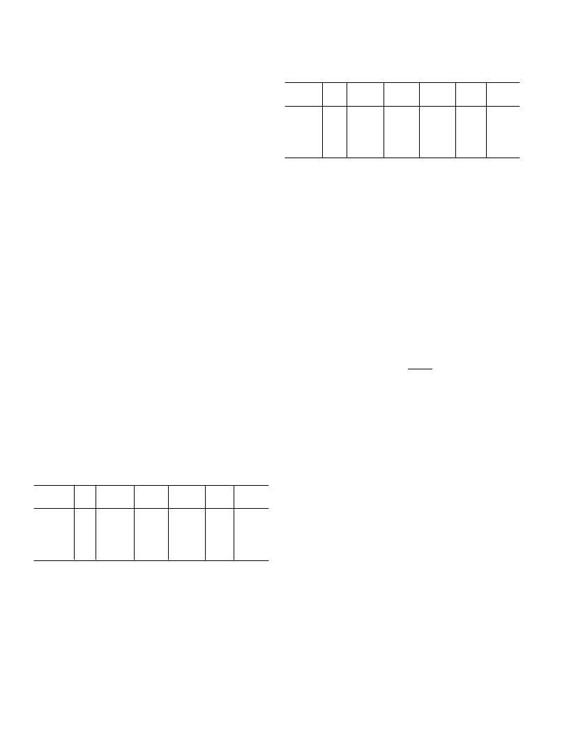
Table II. External Power Calculations (5 V Device)
Pin
Type
# of
Pins
%
Switching
C
f
V
DD2
= P
EXT
Address
MS0
WR
Data
ADDRCLK
15
1
1
32
1
50
0
–
50
–
×
44.7 pF
×
10 MHz
×
44.7 pF
×
10 MHz
×
44.7 pF
×
20 MHz
×
14.7 pF
×
10 MHz
×
4.7 pF
×
25 V
×
25 V
×
25 V
×
25 V
×
25 V
= 0.084 W
= 0.000 W
= 0.022 W
= 0.059 W
= 0.002 W
×
20 MHz
P
EXT
= 0.167 W
Table III. External Power Calculations (3.3 V Device)
Pin
Type
# of
Pins
%
Switching
C
f
V
DD2
= P
EXT
Address
MS0
WR
Data
ADDRCLK
15
1
1
32
1
50
0
–
50
–
×
44.7 pF
×
10 MHz
×
10.9 V = 0.037 W
×
44.7 pF
×
10 MHz
×
10.9 V = 0.000 W
×
44.7 pF
×
20 MHz
×
10.9 V = 0.010 W
×
14.7 pF
×
10 MHz
×
10.9 V = 0.026 W
×
4.7 pF
×
20 MHz
×
10.9 V = 0.001 W
P
EXT
= 0.074 W
A typical power consumption can now be calculated for these
conditions by adding a typical internal power dissipation:
P
TOTAL
= P
EXT
+
(
I
DDIN2
×
5.0
V
)
Note that the conditions causing a worst-case P
EXT
are different
from those causing a worst-case P
INT
. Maximum P
INT
cannot
occur while 100% of the output pins are switching from all ones
to all zeros. Note also that it is not common for an application to
have 100% or even 50% of the outputs switching simultaneously.
TEST CONDITIONS
Output Disable Time
Output pins are considered to be disabled when they stop driv-
ing, go into a high impedance state, and start to decay from
their output high or low voltage. The time for the voltage on the
bus to decay by
V is dependent on the capacitive load, C
L
and
the load current, I
L
. This decay time can be approximated by
the following equation:
t
DECAY
=
C
L
V
I
L
The output disable time t
DIS
is the difference between t
MEASURED
and t
DECAY
as shown in Figure 24. The time t
MEASURED
is the
interval from when the reference signal switches to when the
output voltage decays
V from the measured output high or
output low voltage. t
DECAY
is calculated with test loads C
L
and
I
L
, and with
V equal to 0.5 V.
Output Enable Time
Output pins are considered to be enabled when they have made
a transition from a high impedance state to when they start
driving. The output enable time t
ENA
is the interval from when a
reference signal reaches a high or low voltage level to when the
output has reached a specified high or low trip point, as shown
in the Output Enable/Disable diagram (Figure 24). If multiple
pins (such as the data bus) are enabled, the measurement value
is that of the first pin to start driving.
相關PDF資料 |
PDF描述 |
|---|---|
| ADSP-21061KS-200 | ADSP-2106x SHARC DSP Microcomputer Family |
| ADSP-21061LKB-160 | ADSP-2106x SHARC DSP Microcomputer Family |
| ADSP-21061LKB-176 | ADSP-2106x SHARC DSP Microcomputer Family |
| ADSP-21061LKS-160 | ADSP-2106x SHARC DSP Microcomputer Family |
| ADSP-21061LKS-176 | ADSP-2106x SHARC DSP Microcomputer Family |
相關代理商/技術參數 |
參數描述 |
|---|---|
| ADSP-21061KS-200 | 功能描述:IC DSP CONTROLLER 32BIT 240MQFP RoHS:否 類別:集成電路 (IC) >> 嵌入式 - DSP(數字式信號處理器) 系列:SHARC® 標準包裝:2 系列:StarCore 類型:SC140 內核 接口:DSI,以太網,RS-232 時鐘速率:400MHz 非易失內存:外部 芯片上RAM:1.436MB 電壓 - 輸入/輸出:3.30V 電壓 - 核心:1.20V 工作溫度:-40°C ~ 105°C 安裝類型:表面貼裝 封裝/外殼:431-BFBGA,FCBGA 供應商設備封裝:431-FCPBGA(20x20) 包裝:托盤 |
| ADSP-21061KS-200X | 制造商:未知廠家 制造商全稱:未知廠家 功能描述:32-Bit Digital Signal Processor |
| ADSP-21061KSZ-133 | 功能描述:IC DSP CONTROLLER 32BIT 240MQFP RoHS:是 類別:集成電路 (IC) >> 嵌入式 - DSP(數字式信號處理器) 系列:SHARC® 標準包裝:2 系列:StarCore 類型:SC140 內核 接口:DSI,以太網,RS-232 時鐘速率:400MHz 非易失內存:外部 芯片上RAM:1.436MB 電壓 - 輸入/輸出:3.30V 電壓 - 核心:1.20V 工作溫度:-40°C ~ 105°C 安裝類型:表面貼裝 封裝/外殼:431-BFBGA,FCBGA 供應商設備封裝:431-FCPBGA(20x20) 包裝:托盤 |
| ADSP-21061KSZ-160 | 功能描述:IC DSP CONTROLLER 1MBIT 240MQFP RoHS:是 類別:集成電路 (IC) >> 嵌入式 - DSP(數字式信號處理器) 系列:SHARC® 標準包裝:40 系列:TMS320DM64x, DaVinci™ 類型:定點 接口:I²C,McASP,McBSP 時鐘速率:400MHz 非易失內存:外部 芯片上RAM:160kB 電壓 - 輸入/輸出:3.30V 電壓 - 核心:1.20V 工作溫度:0°C ~ 90°C 安裝類型:表面貼裝 封裝/外殼:548-BBGA,FCBGA 供應商設備封裝:548-FCBGA(27x27) 包裝:托盤 配用:TMDSDMK642-0E-ND - DEVELPER KIT W/NTSC CAMERA296-23038-ND - DSP STARTER KIT FOR TMS320C6416296-23059-ND - FLASHBURN PORTING KIT296-23058-ND - EVAL MODULE FOR DM642TMDSDMK642-ND - DEVELOPER KIT W/NTSC CAMERA |
| ADSP-21061KSZ-200 | 功能描述:IC DSP CONTROLLER 32BIT 240MQFP RoHS:是 類別:集成電路 (IC) >> 嵌入式 - DSP(數字式信號處理器) 系列:SHARC® 標準包裝:40 系列:TMS320DM64x, DaVinci™ 類型:定點 接口:I²C,McASP,McBSP 時鐘速率:400MHz 非易失內存:外部 芯片上RAM:160kB 電壓 - 輸入/輸出:3.30V 電壓 - 核心:1.20V 工作溫度:0°C ~ 90°C 安裝類型:表面貼裝 封裝/外殼:548-BBGA,FCBGA 供應商設備封裝:548-FCBGA(27x27) 包裝:托盤 配用:TMDSDMK642-0E-ND - DEVELPER KIT W/NTSC CAMERA296-23038-ND - DSP STARTER KIT FOR TMS320C6416296-23059-ND - FLASHBURN PORTING KIT296-23058-ND - EVAL MODULE FOR DM642TMDSDMK642-ND - DEVELOPER KIT W/NTSC CAMERA |
發布緊急采購,3分鐘左右您將得到回復。