- 您現(xiàn)在的位置:買(mǎi)賣IC網(wǎng) > PDF目錄374032 > ADSP-2109KP-80 (ANALOG DEVICES INC) Low Cost DSP Microcomputers PDF資料下載
參數(shù)資料
| 型號(hào): | ADSP-2109KP-80 |
| 廠商: | ANALOG DEVICES INC |
| 元件分類: | 數(shù)字信號(hào)處理 |
| 英文描述: | Low Cost DSP Microcomputers |
| 中文描述: | 24-BIT, 20 MHz, OTHER DSP, PQCC68 |
| 封裝: | PLASTIC, LCC-68 |
| 文件頁(yè)數(shù): | 15/36頁(yè) |
| 文件大小: | 333K |
| 代理商: | ADSP-2109KP-80 |
第1頁(yè)第2頁(yè)第3頁(yè)第4頁(yè)第5頁(yè)第6頁(yè)第7頁(yè)第8頁(yè)第9頁(yè)第10頁(yè)第11頁(yè)第12頁(yè)第13頁(yè)第14頁(yè)當(dāng)前第15頁(yè)第16頁(yè)第17頁(yè)第18頁(yè)第19頁(yè)第20頁(yè)第21頁(yè)第22頁(yè)第23頁(yè)第24頁(yè)第25頁(yè)第26頁(yè)第27頁(yè)第28頁(yè)第29頁(yè)第30頁(yè)第31頁(yè)第32頁(yè)第33頁(yè)第34頁(yè)第35頁(yè)第36頁(yè)
ADSP-2104/ADSP-2109
REV. 0
–15–
T E ST CONDIT IONS
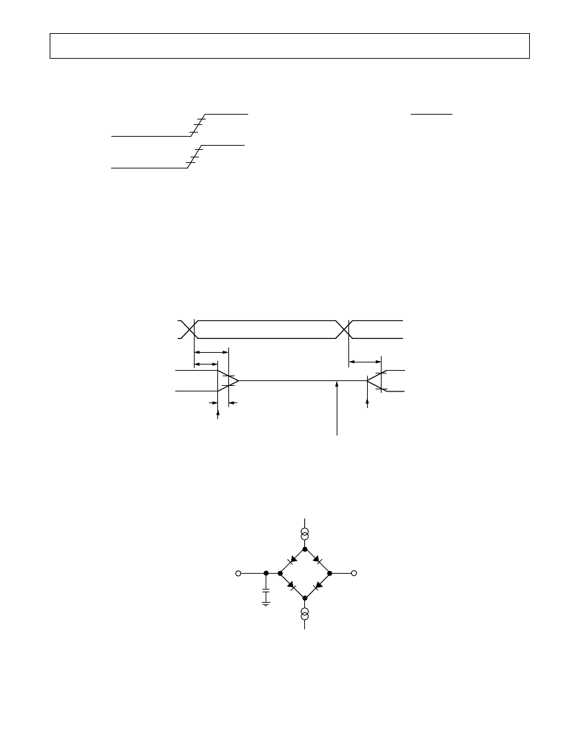
Figure 10 shows voltage reference levels for ac measurements.
3.0V
1.5V
0.0V
2.0V
1.5V
0.8V
INPUT
OUTPUT
Figure 10. Voltage Reference Levels for AC Measurements
(Except Output Enable/Disable)
Output Disable T ime
Output pins are considered to be disabled when they have
stopped driving and started a transition from the measured
output high or low voltage to a high impedance state. T he
output disable time (t
DIS
) is the difference of t
MEASURED
and
t
DECAY
, as shown in Figure 11. T he time t
MEASURED
is the
interval from when a reference signal reaches a high or low
voltage level to when the output voltages have changed by 0.5 V
from the measured output high or low voltage.
T he decay time, t
DECAY
, is dependent on the capacitative load,
C
L
, and the current load, i
L
, on the output pin. It can be
approximated by the following equation:
t
DECAY
=
C
L
×
0.5
V
i
L
from which
t
DIS
=
t
MEASURED
–
t
DECAY
is calculated. If multiple pins (such as the data bus) are dis-
abled, the measurement value is that of the last pin to stop
driving.
Output E nable T ime
Output pins are considered to be enabled when they have made
a transition from a high-impedance state to when they start
driving. T he output enable time (t
E NA
) is the interval from
when a reference signal reaches a high or low voltage level to
when the output has reached a specified high or low trip point,
as shown in Figure 11. If multiple pins (such as the data bus)
are enabled, the measurement value is that of the first pin to
start driving.
SPECIFICATIONS (ADSP-2104/ADSP-2109)
Figure 12. Equivalent Device Loading for AC Measurements
(Except Output Enable/Disable)
2.0V
1.0V
t
ENA
REFERENCE
SIGNAL
OUTPUT
t
DECAY
V
OH
(MEASURED)
OUTPUT STOPS
DRIVING
OUTPUT STARTS
DRIVING
t
DIS
t
MEASURED
V
OL
(MEASURED)
V
OH
(MEASURED) – 0.5V
V
OL
(MEASURED) +0.5V
HIGH-IMPEDANCE STATE.
TEST CONDITIONS CAUSE
THIS VOLTAGE LEVEL TO BE
APPROXIMATELY 1.5V.
V
OH
(MEASURED)
V
OL
(MEASURED)
Figure 11. Output Enable/Disable
TO
OUTPUT
PIN
50pF
+1.5V
I
OH
I
OL
相關(guān)PDF資料 |
PDF描述 |
|---|---|
| ADSP-2109LKP-55 | Low Cost DSP Microcomputers |
| ADSP-2104 | low cost DSP microcomputers |
| ADSP-2109 | Cap-Free, NMOS, 150mA Low Dropout Regulator with Reverse Current Protection |
| ADSP2104 | Low Cost DSP Microcomputers |
| ADSP-2104KP-80 | Low Cost DSP Microcomputers |
相關(guān)代理商/技術(shù)參數(shù) |
參數(shù)描述 |
|---|---|
| ADSP-2109LKP-55 | 制造商:AD 制造商全稱:Analog Devices 功能描述:Low Cost DSP Microcomputers |
| ADSP-2111 | 制造商:AD 制造商全稱:Analog Devices 功能描述:ADSP-2100 Family DSP Microcomputers |
| ADSP-2111BG-52 | 制造商:AD 制造商全稱:Analog Devices 功能描述:ADSP-2100 Family DSP Microcomputers |
| ADSP-2111BG-66 | 制造商:AD 制造商全稱:Analog Devices 功能描述:ADSP-2100 Family DSP Microcomputers |
| ADSP-2111BG-80 | 功能描述:IC DSP CONTROLLER 16BIT 100PGA RoHS:否 類別:集成電路 (IC) >> 嵌入式 - DSP(數(shù)字式信號(hào)處理器) 系列:ADSP-21xx 標(biāo)準(zhǔn)包裝:2 系列:StarCore 類型:SC140 內(nèi)核 接口:DSI,以太網(wǎng),RS-232 時(shí)鐘速率:400MHz 非易失內(nèi)存:外部 芯片上RAM:1.436MB 電壓 - 輸入/輸出:3.30V 電壓 - 核心:1.20V 工作溫度:-40°C ~ 105°C 安裝類型:表面貼裝 封裝/外殼:431-BFBGA,F(xiàn)CBGA 供應(yīng)商設(shè)備封裝:431-FCPBGA(20x20) 包裝:托盤(pán) |
發(fā)布緊急采購(gòu),3分鐘左右您將得到回復(fù)。