- 您現在的位置:買賣IC網 > PDF目錄374033 > ADSP-21366 (Analog Devices, Inc.) Cap-Free, NMOS, 150mA Low Dropout Regulator with Reverse Current Protection PDF資料下載
參數資料
| 型號: | ADSP-21366 |
| 廠商: | Analog Devices, Inc. |
| 元件分類: | 基準電壓源/電流源 |
| 英文描述: | Cap-Free, NMOS, 150mA Low Dropout Regulator with Reverse Current Protection |
| 中文描述: | 無電容,NMOS管,150mA的低壓差穩壓器的反向電流保護 |
| 文件頁數: | 4/54頁 |
| 文件大小: | 559K |
| 代理商: | ADSP-21366 |
第1頁第2頁第3頁當前第4頁第5頁第6頁第7頁第8頁第9頁第10頁第11頁第12頁第13頁第14頁第15頁第16頁第17頁第18頁第19頁第20頁第21頁第22頁第23頁第24頁第25頁第26頁第27頁第28頁第29頁第30頁第31頁第32頁第33頁第34頁第35頁第36頁第37頁第38頁第39頁第40頁第41頁第42頁第43頁第44頁第45頁第46頁第47頁第48頁第49頁第50頁第51頁第52頁第53頁第54頁
Rev. PrA
|
Page 4 of 54
|
September 2004
ADSP-21365/6
Preliminary Technical Data
Independent, Parallel Computation Units
Within each processing element is a set of computational units.
The computational units consist of an arithmetic/logic unit
(ALU), multiplier, and shifter. These units perform all opera-
tions in a single cycle. The three units within each processing
element are arranged in parallel, maximizing computational
throughput. Single multifunction instructions execute parallel
ALU and multiplier operations. In SIMD mode, the parallel
ALU and multiplier operations occur in both processing ele-
ments. These computation units support IEEE 32-bit single-
precision floating-point, 40-bit extended precision floating-
point, and 32-bit fixed-point data formats.
Data Register File
A general-purpose data register file is contained in each pro-
cessing element. The register files transfer data between the
computation units and the data buses, and store intermediate
results. These 10-port, 32-register (16 primary, 16 secondary)
register files, combined with the ADSP-2136x enhanced Har-
vard architecture, allow unconstrained data flow between
computation units and internal memory. The registers in PEX
are referred to as R0-R15 and in PEY as S0-S15.
Single-Cycle Fetch of Instruction and Four Operands
The ADSP-21365/6 features an enhanced Harvard architecture
in which the data memory (DM) bus transfers data and the pro-
gram memory (PM) bus transfers both instructions and data
(see
Figure 1 on page 1
). With the ADSP-21365/6’s separate
program and data memory buses and on-chip instruction cache,
the processor can simultaneously fetch four operands (two over
each data bus) and one instruction (from the cache), all in a sin-
gle cycle.
Instruction Cache
The ADSP-21365/6 includes an on-chip instruction cache that
enables three-bus operation for fetching an instruction and four
data values. The cache is selective—only the instructions whose
fetches conflict with PM bus data accesses are cached. This
cache allows full-speed execution of core, looped operations
such as digital filter multiply-accumulates, and FFT butterfly
processing.
Data Address Generators With Zero-Overhead Hardware
Circular Buffer Support
The ADSP-21365/6’s two data address generators (DAGs) are
used for indirect addressing and implementing circular data
buffers in hardware. Circular buffers allow efficient program-
ming of delay lines and other data structures required in digital
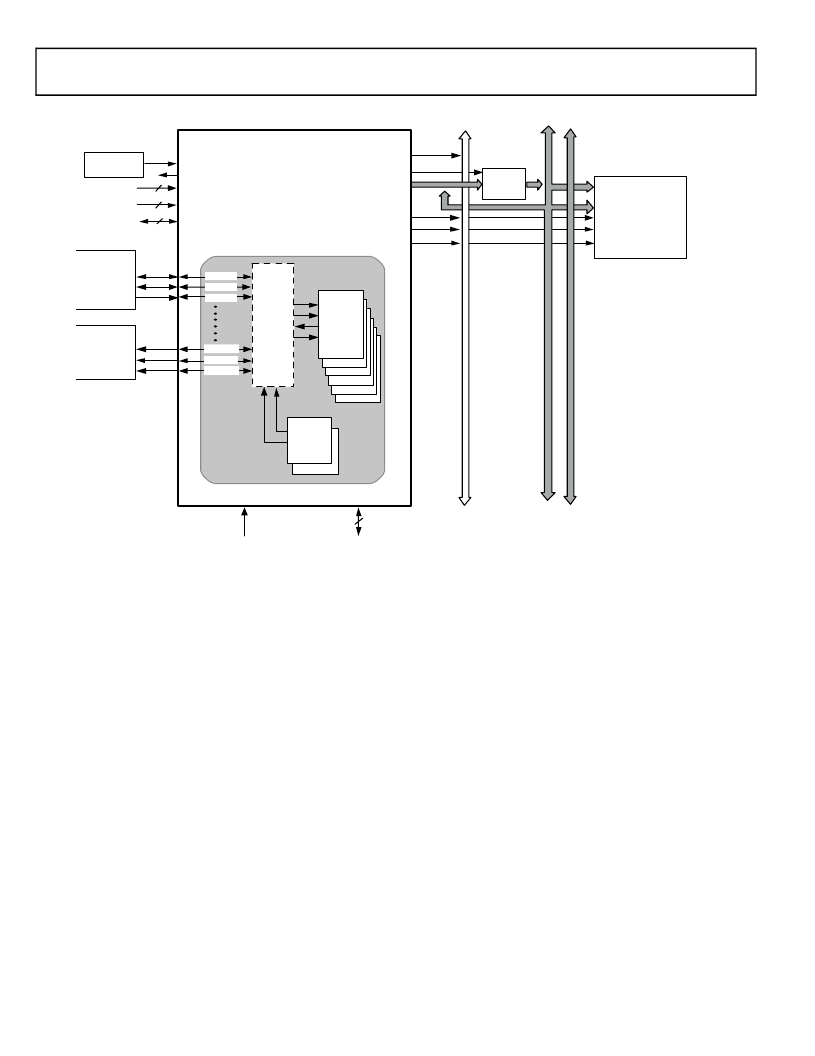
Figure 2. ADSP-21365/6 System Sample Configuration
DAI
SPI
IDP
SRC
SPDIF
SPORT0-5
TIMERS
SCLK0
SFS0
SD0A
SD0B
SRU
DAI_P1
DAI_P2
DAI_P3
DAI_P18
DAI_P19
DAI_P20
DAC
(OPTIONAL)
ADC
(OPTIONAL)
FS
CLK
SDAT
FS
CLK
SDAT
3
CLOCK
FLAG3-1
2
2
CLKIN
XTAL
CLK_CFG1-0
BOOTCFG1-0
ADDR
PARALLEL
PORT
RAM, ROM
BOOT ROM
I/O DEVICE
OE
WE
CS
DATA
RD
WR
CLKOUT
ALE
AD15-0
LATCH
RESET
JTAG
6
ADSP-21365/6
A
D
C
FLAG0
PCGB
PCGA
CLK
FS
相關PDF資料 |
PDF描述 |
|---|---|
| ADSP-21366SKBC-ENG | Cap-Free, NMOS, 150mA Low Dropout Regulator with Reverse Current Protection |
| ADSP-21365 | SHARC Processor |
| ADSP-21365SBBC-ENG | SHARC Processor |
| ADSP-21365SBBCZENG | SHARC Processor |
| ADSP-21365SBSQ-ENG | SHARC Processor |
相關代理商/技術參數 |
參數描述 |
|---|---|
| ADSP-21366BBC-1AA | 功能描述:數字信號處理器和控制器 - DSP, DSC 333 MHz SHARC with on chipRom RoHS:否 制造商:Microchip Technology 核心:dsPIC 數據總線寬度:16 bit 程序存儲器大小:16 KB 數據 RAM 大小:2 KB 最大時鐘頻率:40 MHz 可編程輸入/輸出端數量:35 定時器數量:3 設備每秒兆指令數:50 MIPs 工作電源電壓:3.3 V 最大工作溫度:+ 85 C 封裝 / 箱體:TQFP-44 安裝風格:SMD/SMT |
| ADSP-21366BBCZ-1AA | 功能描述:數字信號處理器和控制器 - DSP, DSC 333 MHz SHARC with on chipRom RoHS:否 制造商:Microchip Technology 核心:dsPIC 數據總線寬度:16 bit 程序存儲器大小:16 KB 數據 RAM 大小:2 KB 最大時鐘頻率:40 MHz 可編程輸入/輸出端數量:35 定時器數量:3 設備每秒兆指令數:50 MIPs 工作電源電壓:3.3 V 最大工作溫度:+ 85 C 封裝 / 箱體:TQFP-44 安裝風格:SMD/SMT |
| ADSP-21366BSWZ-1AA | 功能描述:IC DSP 32BIT 333MHZ EPAD 144LQFP RoHS:是 類別:集成電路 (IC) >> 嵌入式 - DSP(數字式信號處理器) 系列:SHARC® 標準包裝:2 系列:StarCore 類型:SC140 內核 接口:DSI,以太網,RS-232 時鐘速率:400MHz 非易失內存:外部 芯片上RAM:1.436MB 電壓 - 輸入/輸出:3.30V 電壓 - 核心:1.20V 工作溫度:-40°C ~ 105°C 安裝類型:表面貼裝 封裝/外殼:431-BFBGA,FCBGA 供應商設備封裝:431-FCPBGA(20x20) 包裝:托盤 |
| ADSP-21366KBC-1AA | 功能描述:數字信號處理器和控制器 - DSP, DSC 333 MHz SHARC with on chipRom RoHS:否 制造商:Microchip Technology 核心:dsPIC 數據總線寬度:16 bit 程序存儲器大小:16 KB 數據 RAM 大小:2 KB 最大時鐘頻率:40 MHz 可編程輸入/輸出端數量:35 定時器數量:3 設備每秒兆指令數:50 MIPs 工作電源電壓:3.3 V 最大工作溫度:+ 85 C 封裝 / 箱體:TQFP-44 安裝風格:SMD/SMT |
| ADSP-21366KBCZ1AA | 制造商:Analog Devices 功能描述:- Trays |
發布緊急采購,3分鐘左右您將得到回復。