- 您現在的位置:買賣IC網 > PDF目錄374034 > ADSP-2162 (Analog Devices, Inc.) Cap-Free, NMOS, 150mA Low Dropout Regulator with Reverse Current Protection PDF資料下載
參數資料
| 型號: | ADSP-2162 |
| 廠商: | Analog Devices, Inc. |
| 元件分類: | 基準電壓源/電流源 |
| 英文描述: | Cap-Free, NMOS, 150mA Low Dropout Regulator with Reverse Current Protection |
| 中文描述: | 無電容,NMOS管,150mA的低壓差穩壓器的反向電流保護 |
| 文件頁數: | 16/39頁 |
| 文件大小: | 243K |
| 代理商: | ADSP-2162 |
第1頁第2頁第3頁第4頁第5頁第6頁第7頁第8頁第9頁第10頁第11頁第12頁第13頁第14頁第15頁當前第16頁第17頁第18頁第19頁第20頁第21頁第22頁第23頁第24頁第25頁第26頁第27頁第28頁第29頁第30頁第31頁第32頁第33頁第34頁第35頁第36頁第37頁第38頁第39頁
REV. 0
ADSP-216x
SPECIFICATIONS
ADSP-2161/ADSP-2163/ADSP-2165
–16–
TEST CONDITIONS
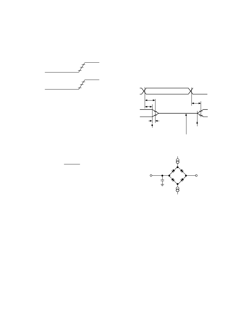
Figure 12 shows voltage reference levels for ac measurements.
1.5V
0.0V
OUTPUT
3.0V
INPUT
1.5V
0.8V
2.0V
Figure 12.VoltageReferenceLevels for AC Measurements
(Except Output Enable/Disable)
Output Disable Time
Output pins are considered to be disabled when they have
stopped driving and started a transition from the measured out-
put high or low voltage to a high impedance state. The output
disable time (t
DIS
) is the difference of t
MEASURED
and t
DECAY
, as
shown in Figure 13. The time t
MEASURED
is the interval from
when a reference signal reaches a high or low voltage level to
when the output voltages have changed by 0.5 V from the mea-
sured output high or low voltage.
The decay time, t
DECAY
, is dependent on the capacitative load,
C
L
, and the current load, i
L
, on the output pin. It can be ap-
proximated by the following equation:
t
C
V
i
DECAY
L
L
=
×
0 5
from which
t
DIS
=
t
MEASURED
–
t
DECAY
is calculated. If multiple pins (such as the data bus) are disabled,
the measurement value is that of the last pin to stop driving.
Output Enable Time
Output pins are considered to be enabled when they have made
a transition from a high-impedance state to when they start
driving. The output enable time (t
ENA
) is the interval from when
a reference signal reaches a high or low voltage level to when the
output has reached a specified high or low trip point, as shown
in Figure 13. If multiple pins (such as the data bus) are enabled,
the measurement value is that of the first pin to start driving.
2.0V
1.0V
t
ENA
REFERENCE
SIGNAL
OUTPUT
t
DECAY
V
(MEASURED)
OUTPUT STOPS
DRIVING
OUTPUT STARTS
DRIVING
t
DIS
t
MEASURED
V
(MEASURED)
V
OH
(MEASURED) – 0.5V
V
OL
(MEASURED) +0.5V
HIGH-IMPEDANCE STATE. TEST CONDITIONS CAUSE
THIS VOLTAGE LEVEL TO BE APPROXIMATELY 1.5V.
V
(MEASURED)
V
(MEASURED)
Figure 13. Output Enable/Disable
TO
OUTPUT
PIN
50pF
+1.5V
I
OH
I
OL
Figure 14. Equivalent Device Loading for AC
Measurements (Except Output Enable/Disable)
相關PDF資料 |
PDF描述 |
|---|---|
| ADSP-2161KS-66 | DSP Microcomputers with ROM |
| ADSP-2163 | Cap-Free, NMOS, 150mA Low Dropout Regulator with Reverse Current Protection |
| ADSP-2164 | Cap-Free, NMOS, 150mA Low Dropout Regulator with Reverse Current Protection |
| ADSP-2165 | Cap-Free, NMOS, 150mA Low Dropout Regulator with Reverse Current Protection |
| ADSP-2166 | Cap-Free, NMOS, 150mA Low Dropout Regulator with Reverse Current Protection |
相關代理商/技術參數 |
參數描述 |
|---|---|
| ADSP-2162BP-40 | 制造商:AD 制造商全稱:Analog Devices 功能描述:ADSP-2100 Family DSP Microcomputers |
| ADSP-2162BS-40 | 制造商:AD 制造商全稱:Analog Devices 功能描述:ADSP-2100 Family DSP Microcomputers |
| ADSP-2162KP-40 | 制造商:AD 制造商全稱:Analog Devices 功能描述:DSP Microcomputers with ROM |
| ADSP-2162KS-40 | 制造商:AD 制造商全稱:Analog Devices 功能描述:ADSP-2100 Family DSP Microcomputers |
| ADSP-2163 | 制造商:AD 制造商全稱:Analog Devices 功能描述:ADSP-2100 Family DSP Microcomputers |
發布緊急采購,3分鐘左右您將得到回復。