- 您現在的位置:買賣IC網 > PDF目錄374034 > ADSP-2171KS-104 (ANALOG DEVICES INC) CAP 4.7PF 50V +/-0.5PF NPO(C0G) SMD-0603 TR-7-PA PDF資料下載
參數資料
| 型號: | ADSP-2171KS-104 |
| 廠商: | ANALOG DEVICES INC |
| 元件分類: | 數字信號處理 |
| 英文描述: | CAP 4.7PF 50V +/-0.5PF NPO(C0G) SMD-0603 TR-7-PA |
| 中文描述: | 24-BIT, 13 MHz, OTHER DSP, PQFP128 |
| 封裝: | PLASTIC, QFP-128 |
| 文件頁數: | 30/52頁 |
| 文件大小: | 664K |
| 代理商: | ADSP-2171KS-104 |
第1頁第2頁第3頁第4頁第5頁第6頁第7頁第8頁第9頁第10頁第11頁第12頁第13頁第14頁第15頁第16頁第17頁第18頁第19頁第20頁第21頁第22頁第23頁第24頁第25頁第26頁第27頁第28頁第29頁當前第30頁第31頁第32頁第33頁第34頁第35頁第36頁第37頁第38頁第39頁第40頁第41頁第42頁第43頁第44頁第45頁第46頁第47頁第48頁第49頁第50頁第51頁第52頁
REV. A
–30–
ADSP-2171/ADSP-2172/ADSP-2173
ADSP-2171/ADSP-2172
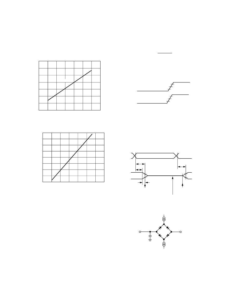
CAPACIT IVE LOADING
Figures 19 and 20 show the capacitive loading characteristics of
the ADSP-2171/ADSP-2172.
R
28
12
4
8
24
16
20
25
150
125
100
75
50
C
L
– pF
V
DD
= 4.5V
Figure 19. Typical Output Rise Time vs. Load Capacitance,
C
L
(at Maximum Ambient Operating Temperature)
+14
+4
–2
+2
+12
+8
+10
25
150
125
100
75
50
C
L
– pF
NOMINAL
V
Figure 20. Typical Output Valid Delay or Hold vs. Load
Capacitance, C
L
(at Maximum Ambient Operating
Temperature)
T E ST CONDIT IONS
Output Disable T ime
Output pins are considered to be disabled when they have
stopped driving and started a transition from the measured out-
put high or low voltage to a high impedance state. T he output
disable time (t
DIS
) is the difference of t
MEASURED
and t
DECAY
, as
shown in the Output Enable/Disable diagram. T he time is the
interval from when a reference signal reaches a high or low volt-
age level to when the output voltages have changed by 0.5 V
from the measured output high or low voltage. T he decay time,
t
DECAY
, is dependent on the capacitative load, C
L
, and the cur-
rent load,
i
L
, on the output pin. It can be approximated by the
following equation:
t
DECAY
=
C
L
· 0.5
V
i
L
from which
t
DIS
=
t
MEASURED
±
t
DECAY
is calculated. If multiple pins (such as the data bus) are dis-
abled, the measurement value is that of the last pin to stop
driving.
3.0V
1.5V
0.0V
2.0V
1.5V
0.3V
INPUT
OUTPUT
Figure 21. Voltage Reference Levels for AC Measure-
ments (Except Output Enable/Disable)
Output E nable T ime
Output pins are considered to be enabled when that have made
a transition from a high-impedance state to when they start driv-
ing. T he output enable time (t
ENA
) is the interval from when a
reference signal reaches a high or low voltage level to when the
output has reached a specified high or low trip point, as shown
in the Output Enable/Disable diagram. If multiple pins (such as
the data bus) are enabled, the measurement value is that of the
first pin to start driving.
2.0V
1.0V
t
ENA
REFERENCE
SIGNAL
OUTPUT
t
DECAY
V
OH
(MEASURED)
OUTPUT STOPS
DRIVING
OUTPUT STARTS
DRIVING
t
DIS
t
MEASURED
V
OL
(MEASURED)
V
OH
(MEASURED) – 0.5V
V
OL
(MEASURED) +0.5V
HIGH-IMPEDANCE STATE. TEST CONDITIONS CAUSE
THIS VOLTAGE LEVEL TO BE APPROXIMATELY 1.5V.
V
OH
(MEASURED)
V
OL
(MEASURED)
Figure 22. Output Enable/Disable
TO
OUTPUT
PIN
50pF
+1.5V
I
OH
I
OL
Figure 23. Equivalent Device Loading for AC Measure-
ments (Including All Fixtures)
相關PDF資料 |
PDF描述 |
|---|---|
| ADSP-2171KS-133 | DSP Microcomputer |
| ADSP-2171KST-104 | DSP Microcomputer |
| ADSP-2171KST-133 | DSP Microcomputer |
| ADSP-2171BST-104 | DSP Microcomputer |
| ADSP-2171BST-133 | DSP Microcomputer |
相關代理商/技術參數 |
參數描述 |
|---|---|
| ADSP-2171KS-133 | 制造商:Analog Devices 功能描述:DSP Fixed-Point 16-Bit 33.33MHz 33MIPS 128-Pin PQFP 制造商:Rochester Electronics LLC 功能描述:16BIT FXD PT PROC 33MIPS - Bulk 制造商:Analog Devices 功能描述:DSP microcomputer 33.33 MHz speed 1 ti |
| ADSP-2171KST-104 | 制造商:Analog Devices 功能描述:DSP Fixed-Point 16-Bit 26MHz 26MIPS 128-Pin TQFP 制造商:Rochester Electronics LLC 功能描述:- Bulk |
| ADSP-2171KST-133 | 制造商:Analog Devices 功能描述:DSP Fixed-Point 16-Bit 33.33MHz 33MIPS 128-Pin TQFP 制造商:Rochester Electronics LLC 功能描述:- Bulk |
| ADSP-2172 | 制造商:AD 制造商全稱:Analog Devices 功能描述:DSP Microcomputer |
| ADSP-2173 | 制造商:AD 制造商全稱:Analog Devices 功能描述:DSP Microcomputer |
發布緊急采購,3分鐘左右您將得到回復。