- 您現在的位置:買賣IC網 > PDF目錄374035 > ADSP-2184LBST-160 (ANALOG DEVICES INC) DSP Microcomputer PDF資料下載
參數資料
| 型號: | ADSP-2184LBST-160 |
| 廠商: | ANALOG DEVICES INC |
| 元件分類: | 數字信號處理 |
| 英文描述: | DSP Microcomputer |
| 中文描述: | 24-BIT, 20 MHz, OTHER DSP, PQFP100 |
| 封裝: | MS-026BED, LQFP-100 |
| 文件頁數: | 27/31頁 |
| 文件大小: | 216K |
| 代理商: | ADSP-2184LBST-160 |
第1頁第2頁第3頁第4頁第5頁第6頁第7頁第8頁第9頁第10頁第11頁第12頁第13頁第14頁第15頁第16頁第17頁第18頁第19頁第20頁第21頁第22頁第23頁第24頁第25頁第26頁當前第27頁第28頁第29頁第30頁第31頁
ADSP-2184L
–27–
REV. 0
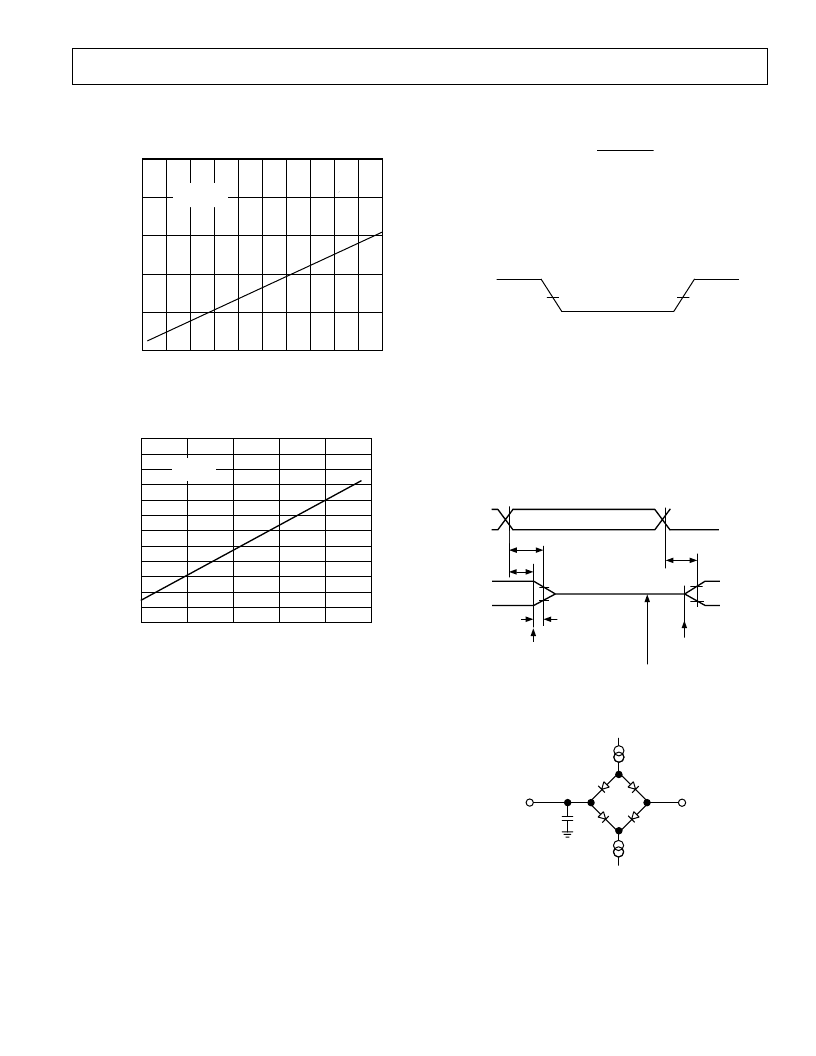
CAPACITIVE LOADING
Figures 22 and 23 show the capacitive loading characteristics of
the ADSP-2184L.
C
L
– pF
25
20
0
0
200
20
R
40
60
80
100
120
140
160
180
15
10
5
V
DD
= 3.0V
T =
1
85
8
C
Figure 22. Typical Output Rise Time vs. Load Capacitance,
C
L
(at Maximum Ambient Operating Temperature)
C
L
– pF
14
0
V
50
100
150
250
200
12
4
2
–2
10
8
NOMINAL
16
18
6
–4
–6
V
DD
= 3.0V
T = +85
8
C
Figure 23. Typical Output Valid Delay or Hold vs. Load
Capacitance, C
L
(at Maximum Ambient Operating
Temperature)
TEST CONDITIONS
Output Disable Time
Output pins are considered to be disabled when they have
stopped driving and started a transition from the measured
output high or low voltage to a high impedance state. The out-
put disable time (t
DIS
) is the difference between t
MEASURED
and
t
DECAY
, as shown in the Output Enable/Disable diagram. The
time is the interval from when a reference signal reaches a high
or low voltage level to when the output voltages have changed
by 0.5 V from the measured output high or low voltage. The
decay time, t
DECAY
, is dependent on the capacitive load, C
L
, and
the current load, i
L
, on the output pin. It can be approximated
by the following equation:
t
DECAY
=
C
L
×
0.5
V
i
L
from which
t
DIS
= t
MEASURED
– t
DECAY
is calculated. If multiple pins (such as the data bus) are dis-
abled, the measurement value is that of the last pin to stop
driving.
1.5V
1.5V
INPUT
OR
OUTPUT
Figure 24. Voltage Reference Levels for AC Measure-
ments (Except Output Enable/Disable)
Output Enable Time
Output pins are considered to be enabled when they have made
a transition from a high-impedance state to when they start
driving. The output enable time (t
ENA
) is the interval from when
a reference signal reaches a high or low voltage level to when the
output has reached a specified high or low trip point, as shown
in the Output Enable/Disable diagram. If multiple pins (such as
the data bus) are enabled, the measurement value is that of the
first pin to start driving.
2.0V
1.0V
t
ENA
REFERENCE
SIGNAL
OUTPUT
t
DECAY
V
(MEASURED)
OUTPUT STOPS
DRIVING
OUTPUT STARTS
DRIVING
t
DIS
t
MEASURED
V
(MEASURED)
V
OH
(MEASURED) – 0.5V
V
OL
(MEASURED) +0.5V
HIGH-IMPEDANCE STATE. TEST CONDITIONS CAUSE
THIS VOLTAGE LEVEL TO BE APPROXIMATELY 1.5V.
V
(MEASURED)
V
(MEASURED)
Figure 25. Output Enable/Disable
TO
OUTPUT
PIN
50pF
+1.5V
I
OH
I
OL
Figure 26. Equivalent Device Loading for AC Measure-
ments (Including All Fixtures)
相關PDF資料 |
PDF描述 |
|---|---|
| ADSP-2184 | LM2941/LM2941C 1A Low Dropout Adjustable Regulator; Package: TO-263; No of Pins: 5; Qty per Container: 45; Container: Rail |
| ADSP-2184BST-160 | DSP Microcomputer |
| ADSP-2184L | LM2941/LM2941C 1A Low Dropout Adjustable Regulator; Package: TO-220; No of Pins: 5; Qty per Container: 45; Container: Rail |
| ADSP-2184NKST-320 | DSP Microcomputer |
| ADSP-2186NKCA-320 | DSP Microcomputer |
相關代理商/技術參數 |
參數描述 |
|---|---|
| ADSP-2184LBSTZ-160 | 功能描述:IC DSP CONTROLLER 16BIT 100LQFP RoHS:是 類別:集成電路 (IC) >> 嵌入式 - DSP(數字式信號處理器) 系列:ADSP-21xx 標準包裝:2 系列:StarCore 類型:SC140 內核 接口:DSI,以太網,RS-232 時鐘速率:400MHz 非易失內存:外部 芯片上RAM:1.436MB 電壓 - 輸入/輸出:3.30V 電壓 - 核心:1.20V 工作溫度:-40°C ~ 105°C 安裝類型:表面貼裝 封裝/外殼:431-BFBGA,FCBGA 供應商設備封裝:431-FCPBGA(20x20) 包裝:托盤 |
| ADSP-2184LBSTZ-1602 | 制造商:AD 制造商全稱:Analog Devices 功能描述:DSP Microcomputer |
| ADSP-2184N | 制造商:AD 制造商全稱:Analog Devices 功能描述:DSP Microcomputer |
| ADSP-2184NBCA-320 | 制造商:Analog Devices 功能描述:DSP Fixed-Point 16-Bit 80MHz 80MIPS 144-Pin CSP-BGA 制造商:Rochester Electronics LLC 功能描述:4K PM/4K DM RAM,16-BIT,80 MIPS, 1.8V - Bulk |
| ADSP-2184NBST-320 | 制造商:Analog Devices 功能描述:DSP Fixed-Point 16-Bit 80MHz 80MIPS 100-Pin LQFP |
發布緊急采購,3分鐘左右您將得到回復。