- 您現在的位置:買賣IC網 > PDF目錄374035 > ADSP-2184N (Analog Devices, Inc.) DSP Microcomputer PDF資料下載
參數資料
| 型號: | ADSP-2184N |
| 廠商: | Analog Devices, Inc. |
| 元件分類: | 數字信號處理 |
| 英文描述: | DSP Microcomputer |
| 中文描述: | DSP微機 |
| 文件頁數: | 10/48頁 |
| 文件大小: | 1571K |
| 代理商: | ADSP-2184N |
第1頁第2頁第3頁第4頁第5頁第6頁第7頁第8頁第9頁當前第10頁第11頁第12頁第13頁第14頁第15頁第16頁第17頁第18頁第19頁第20頁第21頁第22頁第23頁第24頁第25頁第26頁第27頁第28頁第29頁第30頁第31頁第32頁第33頁第34頁第35頁第36頁第37頁第38頁第39頁第40頁第41頁第42頁第43頁第44頁第45頁第46頁第47頁第48頁
ADSP-218xN Series
–10–
REV. 0
Clock Signals
ADSP-218xN series members can be clocked by either a
crystal or a TTL-compatible clock signal.
The CLKIN input cannot be halted, changed during oper-
ation, nor operated below the specified frequency during
normal operation. The only exception is while the processor
is in the power-down state. For additional information, refer
to the
ADSP-218x DSP Hardware Reference
, for detailed
information on this power-down feature.
If an external clock is used, it should be a TTL-compatible
signal running at half the instruction rate. The signal is
connected to the processor’s CLKIN input. When an exter-
nal clock is used, the XTAL pin must be left unconnected.
ADSP-218xN series members use an input clock with a
frequency equal to half the instruction rate; a 40 MHz input
clock yields a 12.5 ns processor cycle (which is equivalent
to 80 MHz). Normally, instructions are executed in a single
processor cycle. All device timing is relative to the internal
instruction clock rate, which is indicated by the CLKOUT
signal when enabled.
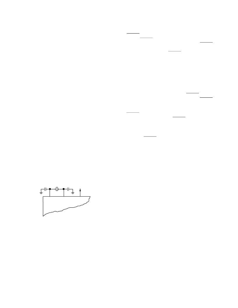
Because ADSP-218xN series members include an on-chip
oscillator circuit, an external crystal may be used. The
crystal should be connected across the CLKIN and XTAL
pins, with two capacitors connected as shown in
Figure 2
.
Capacitor values are dependent on crystal type and should
be specified by the crystal manufacturer. A parallel-
resonant, fundamental frequency, microprocessor-grade
crystal should be used.
A clock output (CLKOUT) signal is generated by the pro-
cessor at the processor’s cycle rate. This can be enabled and
disabled by the CLKODIS bit in the SPORT0 Autobuffer
Control Register.
RESET
The RESET signal initiates a master reset of the ADSP-
218xN. The RESET signal must be asserted during the
power-up sequence to assure proper initialization. RESET
during initial power-up must be held long enough to allow
the internal clock to stabilize. If RESET is activated any time
after power-up, the clock continues to run and does not
require stabilization time.
The power-up sequence is defined as the total time required
for the crystal oscillator circuit to stabilize after a valid V
DD
is applied to the processor, and for the internal phase-locked
loop (PLL) to lock onto the specific crystal frequency. A
minimum of 2000 CLKIN cycles ensures that the PLL has
locked, but does not include the crystal oscillator start-up
time. During this power-up sequence the RESET signal
should be held low. On any subsequent resets, the RESET
signal must meet the minimum pulse-width specification
(t
RSP
).
The RESET input contains some hysteresis; however, if an
RC circuit is used to generate the RESET signal, the use of
an external Schmitt trigger is recommended.
The master reset sets all internal stack pointers to the empty
stack condition, masks all interrupts, and clears the MSTAT
register. When RESET is released, if there is no pending
bus request and the chip is configured for booting, the boot-
loading sequence is performed. The first instruction is
fetched from on-chip program memory location 0x0000
once boot loading completes.
POWER SUPPLIES
ADSP-218xN series members have separate power supply
connections for the internal (V
DDINT
) and external (V
DDEXT
)
power supplies. The internal supply must meet the 1.8 V
requirement. The external supply can be connected to a
1.8 V, 2.5 V, or 3.3 V supply. All external supply pins must
be connected to the same supply. All input and I/O pins can
tolerate input voltages up to 3.6 V, regardless of the external
supply voltage. This feature provides maximum flexibility
in mixing 1.8 V, 2.5 V, or 3.3 V components.
Figure 2. External Crystal Connections
CLKIN
CLKOUT
XTAL
DSP
相關PDF資料 |
PDF描述 |
|---|---|
| ADSP-2187N | DSP Microcomputer |
| ADSP-2188 | Cap-Free, NMOS, 150mA Low Dropout Regulator with Reverse Current Protection |
| ADSP-2188NBCA-320 | Cap-Free, NMOS, 150mA Low Dropout Regulator with Reverse Current Protection |
| ADSP-2188NBST-320 | Cap-Free, NMOS, 150mA Low Dropout Regulator with Reverse Current Protection |
| ADSP-218XNSERIES | DSP Microcomputer |
相關代理商/技術參數 |
參數描述 |
|---|---|
| ADSP-2184NBCA-320 | 制造商:Analog Devices 功能描述:DSP Fixed-Point 16-Bit 80MHz 80MIPS 144-Pin CSP-BGA 制造商:Rochester Electronics LLC 功能描述:4K PM/4K DM RAM,16-BIT,80 MIPS, 1.8V - Bulk |
| ADSP-2184NBST-320 | 制造商:Analog Devices 功能描述:DSP Fixed-Point 16-Bit 80MHz 80MIPS 100-Pin LQFP |
| ADSP-2184NBSTZ-320 | 功能描述:IC DSP CONTROLLER 16BIT 100LQFP RoHS:是 類別:集成電路 (IC) >> 嵌入式 - DSP(數字式信號處理器) 系列:ADSP-21xx 標準包裝:2 系列:StarCore 類型:SC140 內核 接口:DSI,以太網,RS-232 時鐘速率:400MHz 非易失內存:外部 芯片上RAM:1.436MB 電壓 - 輸入/輸出:3.30V 電壓 - 核心:1.20V 工作溫度:-40°C ~ 105°C 安裝類型:表面貼裝 封裝/外殼:431-BFBGA,FCBGA 供應商設備封裝:431-FCPBGA(20x20) 包裝:托盤 |
| ADSP-2184NKCA-320 | 功能描述:IC DSP 16BIT 80MHZ 144CSPBGA RoHS:否 類別:集成電路 (IC) >> 嵌入式 - DSP(數字式信號處理器) 系列:ADSP-21xx 標準包裝:2 系列:StarCore 類型:SC140 內核 接口:DSI,以太網,RS-232 時鐘速率:400MHz 非易失內存:外部 芯片上RAM:1.436MB 電壓 - 輸入/輸出:3.30V 電壓 - 核心:1.20V 工作溫度:-40°C ~ 105°C 安裝類型:表面貼裝 封裝/外殼:431-BFBGA,FCBGA 供應商設備封裝:431-FCPBGA(20x20) 包裝:托盤 |
| ADSP2184NKST320 | 制造商:AD 功能描述:New |
發布緊急采購,3分鐘左右您將得到回復。