- 您現在的位置:買賣IC網 > PDF目錄374038 > ADT7461ARM (ANALOG DEVICES INC) 【1∑C Temperature Monitor with Series Resistance Cancellation PDF資料下載
參數資料
| 型號: | ADT7461ARM |
| 廠商: | ANALOG DEVICES INC |
| 元件分類: | 模擬信號調理 |
| 英文描述: | 【1∑C Temperature Monitor with Series Resistance Cancellation |
| 中文描述: | SPECIALTY ANALOG CIRCUIT, PDSO8 |
| 封裝: | MO-187-AA, MSOP-8 |
| 文件頁數: | 15/24頁 |
| 文件大小: | 854K |
| 代理商: | ADT7461ARM |
ADT7461
serial bus in a single read or write operation is limited only
by what the master and slave devices can handle.
3.
When all data bytes have been read or written, stop condi-
tions are established. In write mode, the master will pull the
data line high during the tenth clock pulse to assert a STOP
condition. In read mode, the master device will override
the acknowledge bit by pulling the data line high during
the low period before the ninth clock pulse. This is known
as No Acknowledge. The master will then take the data line
low during the low period before the tenth clock pulse,
then high during the tenth clock pulse to assert a STOP
condition.
Any number of bytes of data may be transferred over the serial
bus in one operation, but it is not possible to mix read and write
in one operation because the type of operation is determined at
the beginning and cannot subsequently be changed without
starting a new operation. In the case of the ADT7461, write
operations contain either one or two bytes, while read opera-
tions contain one byte.
To write data to one of the device data registers or to read
data from it, the address pointer register must be set so that the
correct data register is addressed. The first byte of a write opera-
tion always contains a valid address that is stored in the address
pointer register. If data is to be written to the device, the write
operation contains a second data byte that is written to the
register selected by the address pointer register.
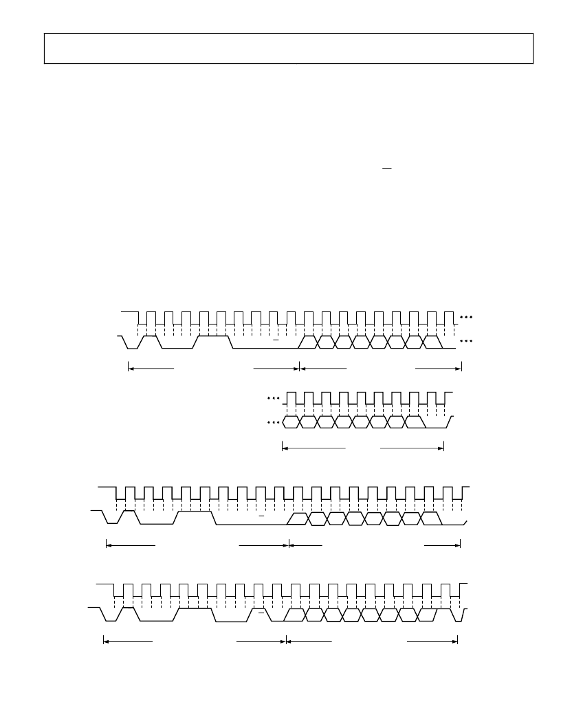
This is illustrated in
the bus followed by R/W set to 0. This is followed by two data
bytes. The first data byte is the address of the internal data
register to be written to, which is stored in the address pointer
register. The second data byte is the data to be written to the
internal data register.
. The device address is sent over
Figure 15
Figure 15. Writing a Register Address to the Address Pointer Register, then Writing Data to the Selected Register
0
A6
1
9
1
A5
A4
A3
A2
A1
A0
R/W
D7
D6
D5
D4
D3
D2
D1
D0
SCLK
SDAT
9
A
START BY
MASTER
ACK. BY
ADT7461
FRAME 1
SERIAL BUS ADDRESS BYTE
FRAME 2
ADDRESS POINTER REGISTER BYTE
FRAME 3
DATA BYTE
SCLK (CONTINUED)
SDATA (CONTINUED)
ACK. BY
ADT7461
ACK. BY
ADT7461
STOP BY
MASTER
9
1
D7
D6
D5
D4
D3
D2
D1
D0
0
SCLK
SDATA
START BY
MASTER
ACK. BY
ADT7461
ACK. BY
ADT7461
STOP BY
MASTER
FRAME 1
SERIAL BUS ADDRESS BYTE
FRAME 2
ADDRESS POINTER REGISTER BYTE
1
9
1
A6
A5
A4
A3
A2
A1
A0
R/W
D7
D6
D5
D4
D3
D2
D1
D0
9
Figure 16. Writing to the Address Pointer Register Only
0
SCLK
SDATA
START BY
MASTER
ACK. BY
ADT7461
FRAME 1
SERIAL BUS ADDRESS BYTE
FRAME 2
DATA BYTE FROM ADT7461
ACK. BY
ADT7461
STOP BY
MASTER
1
9
1
9
A6
A5
A4
A3
A2
A1
A0
R/W
D7
D6
D5
D4
D3
D2
D1
D0
Figure 17. Reading from a Previously Selected Register
Rev. 0 | Page 15 of 24
相關PDF資料 |
PDF描述 |
|---|---|
| ADT7461ARM-REEL | 【1∑C Temperature Monitor with Series Resistance Cancellation |
| ADT7461ARM-REEL7 | 【1∑C Temperature Monitor with Series Resistance Cancellation |
| ADT7463 | dB COOL Remote Thermal Controller and Voltage Monitor |
| ADT7463ARQ | dB COOL Remote Thermal Controller and Voltage Monitor |
| ADT7466 | dBCool Remote Thermal Controller and Voltage Monitor |
相關代理商/技術參數 |
參數描述 |
|---|---|
| ADT7461ARM2-2 | 制造商:Analog Devices 功能描述: |
| ADT7461ARM-REEL | 制造商:Rochester Electronics LLC 功能描述:+/-1C TDM SRC EXT TEMP RANGE I.C. - Tape and Reel |
| ADT7461ARM-REEL7 | 制造商:Rochester Electronics LLC 功能描述:+/-1C TDM SRC EXT TEMP RANGE I.C. - Tape and Reel |
| ADT7461ARMZ | 功能描述:板上安裝溫度傳感器 EXT TMP RGE IC 1C TDM SRC RoHS:否 制造商:Omron Electronics 輸出類型:Digital 配置: 準確性:+/- 1.5 C, +/- 3 C 溫度閾值: 數字輸出 - 總線接口:2-Wire, I2C, SMBus 電源電壓-最大:5.5 V 電源電壓-最小:4.5 V 最大工作溫度:+ 50 C 最小工作溫度:0 C 關閉: 安裝風格: 封裝 / 箱體: 設備功能:Temperature and Humidity Sensor |
| ADT7461ARMZ | 制造商:ON Semiconductor 功能描述:Temperature Sensor IC |
發布緊急采購,3分鐘左右您將得到回復。