- 您現在的位置:買賣IC網 > PDF目錄374038 > ADT7518ARQ-REEL7 (Analog Devices, Inc.) SPI/I2C Compatible, Temperature Sensor, 4-Channel ADC and Quad Voltage Output DAC PDF資料下載
參數資料
| 型號: | ADT7518ARQ-REEL7 |
| 廠商: | Analog Devices, Inc. |
| 元件分類: | 溫度/濕度傳感器 |
| 英文描述: | SPI/I2C Compatible, Temperature Sensor, 4-Channel ADC and Quad Voltage Output DAC |
| 中文描述: | SPI/I2C兼容,溫度傳感器,4通道ADC和四路電壓輸出DAC |
| 文件頁數: | 19/40頁 |
| 文件大小: | 1217K |
| 代理商: | ADT7518ARQ-REEL7 |
第1頁第2頁第3頁第4頁第5頁第6頁第7頁第8頁第9頁第10頁第11頁第12頁第13頁第14頁第15頁第16頁第17頁第18頁當前第19頁第20頁第21頁第22頁第23頁第24頁第25頁第26頁第27頁第28頁第29頁第30頁第31頁第32頁第33頁第34頁第35頁第36頁第37頁第38頁第39頁第40頁
ADT7518
DAC Reference Inputs
There is an input reference pin for the DACs. This reference
input is buffered (see Figure 40).
Rev. A | Page 19 of 40
V
REF
and this can be increased to 0 V to 2 V
REF
. Increasing the
output voltage span to 2 V
REF
can be done by setting D0 = 1 for
DAC A (internal temperature sensor) and D1 = 1 for DAC B
(external temperature sensor) in the DAC configuration register
(Address 1Bh).
The advantage with the buffered input is the high impedance it
presents to the voltage source driving it. The user can have an
external reference voltage as low as 1 V and as high as V
DD
. The
restriction of 1 V is due to the footroom of the reference buffer.
The output voltage is capable of tracking a maximum temp-
erature range of –128°C to +127°C, but the default setting is
–40°C to +127°C. If the output voltage range is 0 V to V
REF
-IN
(V
REF
-IN = 2.25 V), then this corresponds to 0 V representing
–40°C, and 1.48 V representing +127°C. This, of course, will
give an upper deadband between 1.48 V and V
REF
.
The LDAC configuration register controls the option to select
between internal and external voltage references. The default
setting is for external reference selected.
Output Amplifier
The output buffer amplifier can generate output voltages to
within 1 mV of either rail. Its actual range depends on the value
of V
REF
, gain, and offset error.
The internal and external analog temperature offset registers
can be used to vary this upper deadband and, consequently, the
temperature that 0 V corresponds to. Table 6 and Table 7 give
examples of how this is done using a DAC output voltage span
of V
REF
and 2 V
REF
, respectively. Simply write in the temperature
value, in twos complement format, at which 0 V is to start. For
example, if using the DAC A output and 0 V to start at –40°C,
program D8h into the internal analog temperature offset reg-
ister (Address 21h). This is an 8-bit register and has a temp-
erature offset resolution of only 1°C for all device models. Use
the formulas following the tables to determine the value to
program into the offset registers.
Table 6. Thermal Voltage Output (0 V to V
REF
)
If a gain of 1 is selected (Bits 0 to 3 of the DAC configuration
register = 0), the output range is 0.001 V to V
REF
.
If a gain of 2 is selected (Bits 0 to 3 of the DAC configuration
register = 1), the output range is 0.001 V to 2 V
REF
. Because of
clamping, however, the maximum output is limited to V
DD
0.001 V.
The output amplifier can drive a load of 4.7 k to GND or V
DD
,
in parallel with 200 pF to GND or V
DD
(see Figure 5). The
source and sink capabilities of the output amplifier can be seen
in the plot of Figure 16.
O/P Voltage (V)
0
0.5
1
1.12
1.47
1.5
2
2.25
Default °C
–40
+17
+73
+87
+127
UDB
UDB
UDB
Max °C
–128
–71
–15
–1
+39
+42
+99
+127
Sample °C
0
+56
+113
+127
UDB
UDB
UDB
UDB
The slew rate is 0.7 V/μs with a half-scale settling time to
±0.5 LSB (at 8 bits) of 6 μs.
Thermal Voltage Output
The ADT7518 can output voltages that are proportional to
temperature. DAC A output can be configured to represent the
temperature of the internal sensor while DAC B output can be
configured to represent the external temperature sensor. Bits C5
and C6 of the Control Configuration 3 register select the temp-
erature proportional output voltage. Each time a temperature
measurement is taken, the DAC output is updated. The output
resolution for the ADT7518 is 8 bits with a 1°C change corres-
ponding to 1 LSB change. The default output range is 0 V to
Upper deadband has been reached. DAC output is not capable of
increasing. See Fig
.
ure 9
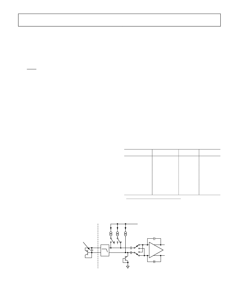
C1
D–
D+
LFILTER
f
C
= 65kHz
BIAS
DIODE
V
DD
TO ADC
V
OUT+
V
OUT–
REMOTE
SENSING
TRANSISTOR
(2N3906)
OPTIONAL CAPACITOR, UP TO
3nF MAX. CAN BE ADDED TO
NOISE REJECTION IN NOISY
ENVIRONMENTS
I
N
×
I
I
BIAS
0
Figure 41. Signal Conditioning for External Diode Temperature Sensor
相關PDF資料 |
PDF描述 |
|---|---|
| ADT7518ARQZ | SPI/I2C Compatible, Temperature Sensor, 4-Channel ADC and Quad Voltage Output DAC |
| ADT7518ARQZ-REEL | SPI/I2C Compatible, Temperature Sensor, 4-Channel ADC and Quad Voltage Output DAC |
| ADT7518ARQZ-REEL7 | SPI/I2C Compatible, Temperature Sensor, 4-Channel ADC and Quad Voltage Output DAC |
| ADUC7020BCP62 | Precision Analog Microcontroller 12-bit Analog I/O, ARM7TDMI MCU |
| ADUC7021ACP32 | Precision Analog Microcontroller 12-bit Analog I/O, ARM7TDMI MCU |
相關代理商/技術參數 |
參數描述 |
|---|---|
| ADT7518ARQ-U3 | 制造商:Analog Devices 功能描述:- Bulk |
| ADT7518ARQZ | 功能描述:IC SENSOR TEMP QD ADC/DAC 16QSOP RoHS:是 類別:集成電路 (IC) >> PMIC - 熱管理 系列:- 標準包裝:2,500 系列:SilentSense™ 功能:溫度監控系統(傳感器) 傳感器類型:內部和外部 感應溫度:-55°C ~ 125°C,外部傳感器 精確度:±2°C 本地(最大),±3°C 遠程(最大) 拓撲:ADC(三角積分型),比較器,寄存器庫 輸出類型:I²C?/SMBus? 輸出警報:是 輸出風扇:是 電源電壓:2.7 V ~ 5.5 V 工作溫度:-55°C ~ 125°C 安裝類型:表面貼裝 封裝/外殼:8-TSSOP,8-MSOP(0.118",3.00mm 寬) 供應商設備封裝:8-MSOP 包裝:帶卷 (TR) 其它名稱:MIC284-2BMMTRMIC284-2BMMTR-ND |
| ADT7518ARQZ-REEL | 制造商:Analog Devices 功能描述:Temp Sensor Analog Serial (4-Wire, SPI, I2C) 16-Pin QSOP T/R |
| ADT7518ARQZ-REEL7 | 制造商:Analog Devices 功能描述:Temp Sensor Analog Serial (4-Wire, SPI, I2C) 16-Pin QSOP T/R |
| ADT7519 | 制造商:AD 制造商全稱:Analog Devices 功能描述:SPI-/I2C-Compatible, Temperature Sensor,4-Channel ADC and Quad Voltage Output |
發布緊急采購,3分鐘左右您將得到回復。