- 您現在的位置:買賣IC網 > PDF目錄374038 > ADT7519ARQZ1-REEL7 (Analog Devices, Inc.) SPI/I2C Compatible, Temperature Sensor, Four Channel ADC and Quad Voltage Output DAC PDF資料下載
參數資料
| 型號: | ADT7519ARQZ1-REEL7 |
| 廠商: | Analog Devices, Inc. |
| 元件分類: | 溫度/濕度傳感器 |
| 英文描述: | SPI/I2C Compatible, Temperature Sensor, Four Channel ADC and Quad Voltage Output DAC |
| 中文描述: | SPI/I2C兼容,溫度傳感器,四通道ADC和四路電壓輸出DAC |
| 文件頁數: | 33/44頁 |
| 文件大小: | 1350K |
| 代理商: | ADT7519ARQZ1-REEL7 |
第1頁第2頁第3頁第4頁第5頁第6頁第7頁第8頁第9頁第10頁第11頁第12頁第13頁第14頁第15頁第16頁第17頁第18頁第19頁第20頁第21頁第22頁第23頁第24頁第25頁第26頁第27頁第28頁第29頁第30頁第31頁第32頁當前第33頁第34頁第35頁第36頁第37頁第38頁第39頁第40頁第41頁第42頁第43頁第44頁
ADT7516/ADT7517/ADT7519
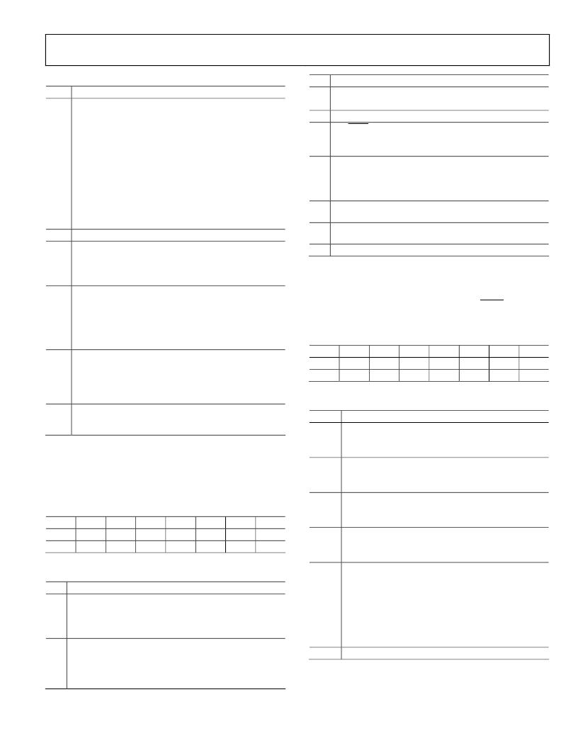
Table 40.
Bit
C2:0 In single-channel mode, these bits select between V
DD
,
the internal temperature sensor, external temperature
sensor/AIN1, AIN2, AIN3, and AIN4 for conversion. The
default is V
DD
.
000 = V
DD
.
001 = Internal temperature sensor.
010 = External temperature sensor/AIN1. (Bits C1:C2 of
the Control Configuration 1 register affect this selection).
011 = AIN2.
100 = AIN3.
101 = AIN4.
110–111 = Reserved.
C3
Reserved.
C4
Selects between single-channel and round robin conver-
sion cycle. The default is round robin.
0 = Round robin.
1 = Single channel.
C5
Default condition is to average every measurement on all
channels 16 times. This bit disables this averaging.
Channels affected are temperature, analog inputs, and
V
DD
.
0 = Enable averaging.
1 = Disable averaging.
C6
SMBus timeout on the serial clock puts a 25 ms limit on
the pulse width of the clock, ensuring that a fault on the
master SCL does not lock up the SDA line.
0 = Disable SMBus timeout.
1 = Enable SMBus timeout.
C7
Software Reset. Setting this bit to 1 causes a software
reset. All registers and DAC outputs will reset to their
default settings.
Control Configuration 3 Register (Read/Write) [Add. =
1Ah]
This configuration register is an 8-bit read/write register that is
used to set up some of the operating modes of the ADT7516/
ADT7517/ADT7519.
Table 41. Control Configuration 3
D7
D6
D5
D4
C7
C6
C5
C4
0*
0*
0*
0*
Rev. A | Page 33 of 44
Function
D3
C3
0*
D2
C2
0*
D1
C1
0*
D0
C0
0*
*Default settings at power-up.
Table 42.
Bit Function
C0
Selects between fast and slow ADC conversion speeds.
0 = ADC clock at 1.4 kHz.
1 = ADC clock at 22.5 kHz. D+ and D– analog filters are
disabled.
C1
On the ADT7516 and ADT7517, this bit selects between 8-
bit and 10-bit DAC output resolution on the thermal
voltage output feature. The default is 8 bits. This bit has no
effect on the ADT7519 output because this part has only
an 8-bit DAC. For the ADT7519, write 0 to this bit.
Bit
Function
0 = 8-bit resolution.
1 = 10-bit resolution.
Reserved. Write 0 only.
0 = LDAC pin controls updating of DAC outputs.
1 = DAC configuration register and LDAC configu ration
register control updating of DAC outputs.
Selects the ADC reference to be either internal V
REF
or V
DD
for analog inputs.
0 = Internal V
REF.
1 = V
DD
.
Setting this bit selects DAC A voltage output to be
proportional to the internal temperature measurement.
Setting this bit selects DAC B voltage output to be
proportional to the external temperature measurement.
Reserved. Write 0 only.
C2
C3
C4
C5
C6
C7
DAC Configuration Register (Read/Write) [Add. = 1Bh]
This configuration register is an 8-bit read/write register that is
used to control the output ranges of all four DACs and also to
control the loading of the DAC registers if the LDAC pin is
disabled (Bit C3 = 1, Control Configuration 3 register).
Table 43. DAC Configuration
D7
D6
D7
D6
0*
0*
D5
D5
0*
D4
D4
0*
D3
D3
0*
D2
D2
0*
D1
D1
0*
D0
D0
0*
*Default settings at power-up.
Table 44.
Bit
Function
D0
Selects the output range of DAC A.
0 = 0 V to V
REF
.
1 = 0 V to 2V
REF
.
D1
Selects the output range of DAC B.
0 = 0 V to V
REF
.
1 = 0 V to 2V
REF
.
D2
Selects the output range of DAC C.
0 = 0 V to V
REF
.
1 = 0 V to 2V
REF
.
D3
Selects the output range of DAC D.
0 = 0 V to V
REF
.
1 = 0 V to 2V
REF
.
D5:D
4
command that updates that DAC only.
01 = MSB write to DAC B or DAC D register generates
LDAC command that updates DACs A, B or DACs C, D,
respectively.
10 = MSB write to DAC D register generates LDAC
command that updates all four DACs.
11 = LDAC command generated from LDAC register.
D6:D7
Reserved. Write 0s only.
00 = MSB write to any DAC register generates LDAC
相關PDF資料 |
PDF描述 |
|---|---|
| ADT7516ARQ | SPI/I2C Compatible, Temperature Sensor, Four Channel ADC and Quad Voltage Output DAC |
| ADT7517ARQ | SPI/I2C Compatible, Temperature Sensor, Four Channel ADC and Quad Voltage Output DAC |
| ADT7519ARQ | SPI/I2C Compatible, Temperature Sensor, Four Channel ADC and Quad Voltage Output DAC |
| ADT7519ARQ-REEL | SPI/I2C Compatible, Temperature Sensor, Four Channel ADC and Quad Voltage Output DAC |
| ADT7517ARQ-REEL | SPI/I2C Compatible, Temperature Sensor, Four Channel ADC and Quad Voltage Output DAC |
相關代理商/技術參數 |
參數描述 |
|---|---|
| ADT7519ARQZ-REEL | 功能描述:IC SENSOR TEMP QD ADC/DAC 16QSOP RoHS:是 類別:集成電路 (IC) >> PMIC - 熱管理 系列:- 標準包裝:2,500 系列:SilentSense™ 功能:溫度監控系統(傳感器) 傳感器類型:內部和外部 感應溫度:-55°C ~ 125°C,外部傳感器 精確度:±2°C 本地(最大),±3°C 遠程(最大) 拓撲:ADC(三角積分型),比較器,寄存器庫 輸出類型:I²C?/SMBus? 輸出警報:是 輸出風扇:是 電源電壓:2.7 V ~ 5.5 V 工作溫度:-55°C ~ 125°C 安裝類型:表面貼裝 封裝/外殼:8-TSSOP,8-MSOP(0.118",3.00mm 寬) 供應商設備封裝:8-MSOP 包裝:帶卷 (TR) 其它名稱:MIC284-2BMMTRMIC284-2BMMTR-ND |
| ADT7519ARQZ-REEL7 | 功能描述:IC SENSOR TEMP QD ADC/DAC 16QSOP RoHS:是 類別:集成電路 (IC) >> PMIC - 熱管理 系列:- 標準包裝:2,500 系列:SilentSense™ 功能:溫度監控系統(傳感器) 傳感器類型:內部和外部 感應溫度:-55°C ~ 125°C,外部傳感器 精確度:±2°C 本地(最大),±3°C 遠程(最大) 拓撲:ADC(三角積分型),比較器,寄存器庫 輸出類型:I²C?/SMBus? 輸出警報:是 輸出風扇:是 電源電壓:2.7 V ~ 5.5 V 工作溫度:-55°C ~ 125°C 安裝類型:表面貼裝 封裝/外殼:8-TSSOP,8-MSOP(0.118",3.00mm 寬) 供應商設備封裝:8-MSOP 包裝:帶卷 (TR) 其它名稱:MIC284-2BMMTRMIC284-2BMMTR-ND |
| ADT7519ARZQ | 制造商:Analog Devices 功能描述: |
| ADT75ARM | 制造商:Rochester Electronics LLC 功能描述: 制造商:Analog Devices 功能描述: |
| ADT75ARM-REEL | 制造商:Rochester Electronics LLC 功能描述: 制造商:Analog Devices 功能描述: |
發布緊急采購,3分鐘左右您將得到回復。