- 您現在的位置:買賣IC網 > PDF目錄374038 > ADUC7020BCP62 (ANALOG DEVICES INC) Precision Analog Microcontroller 12-bit Analog I/O, ARM7TDMI MCU PDF資料下載
參數資料
| 型號: | ADUC7020BCP62 |
| 廠商: | ANALOG DEVICES INC |
| 元件分類: | 微控制器/微處理器 |
| 英文描述: | Precision Analog Microcontroller 12-bit Analog I/O, ARM7TDMI MCU |
| 中文描述: | 32-BIT, FLASH, 45.5 MHz, MICROCONTROLLER, QCC40 |
| 封裝: | 6 X 6 MM, MO-220VJJD-2, LFCSP-40 |
| 文件頁數: | 12/80頁 |
| 文件大小: | 840K |
| 代理商: | ADUC7020BCP62 |
第1頁第2頁第3頁第4頁第5頁第6頁第7頁第8頁第9頁第10頁第11頁當前第12頁第13頁第14頁第15頁第16頁第17頁第18頁第19頁第20頁第21頁第22頁第23頁第24頁第25頁第26頁第27頁第28頁第29頁第30頁第31頁第32頁第33頁第34頁第35頁第36頁第37頁第38頁第39頁第40頁第41頁第42頁第43頁第44頁第45頁第46頁第47頁第48頁第49頁第50頁第51頁第52頁第53頁第54頁第55頁第56頁第57頁第58頁第59頁第60頁第61頁第62頁第63頁第64頁第65頁第66頁第67頁第68頁第69頁第70頁第71頁第72頁第73頁第74頁第75頁第76頁第77頁第78頁第79頁第80頁
ADuC702x Series
Preliminary Technical Data
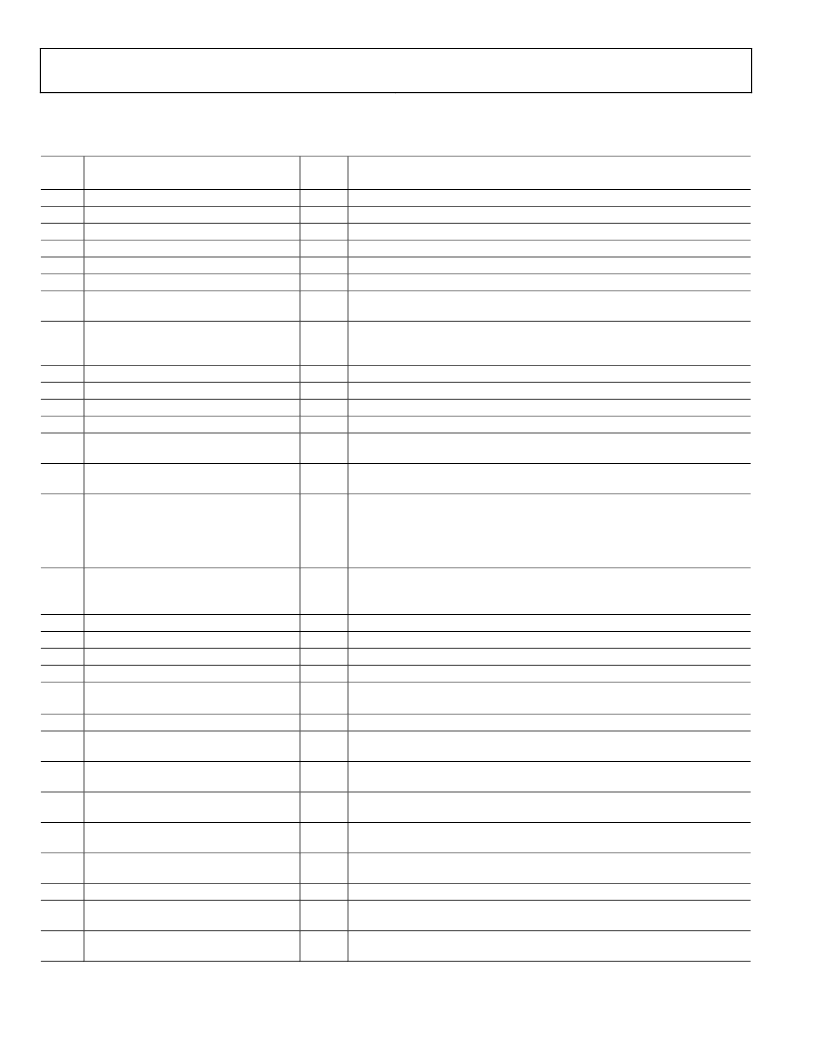
PIN FUNCTION DESCRIPTIONS – ADUC7024/ADUC7025
Table 4. Pin Function Descriptions
Rev. PrB | Page 12 of 80
Pin#
Mnemonic
Type
*
Function
1
2
3
4
5
6
ADC4
ADC5
ADC6
ADC7
ADC8
ADC9
I
I
I
I
I
I
Single-ended or differential Analog input 4
Single-ended or differential Analog input 5
Single-ended or differential Analog input 6
Single-ended or differential Analog input 7
Single-ended or differential Analog input 8
Single-ended or differential Analog input 9
Ground voltage reference for the ADC. For optimal performance the analog
power supply should be separated from IOGND and DGND
Bias point or Negative Analog Input of the ADC in pseudo differential mode.
Must be connected to the ground of the signal to convert. This bias point
must be between 0V and 1V
DAC0 Voltage Output / Single-ended or differential Analog input 12
DAC1 Voltage Output / Single-ended or differential Analog input 13
JTAG Test Port Input - Test Mode Select. Debug and download access
JTAG Test Port Input – Test Data In. Debug and download access
General Purpose Input-Output Port 4.6/ Programmable Logic Array Output
Element 14
General Purpose Input-Output Port 4.7/ Programmable Logic Array Output
Element 15
Multifunction I/O pin:
Boot Mode. The ADuC7024/ADuC7025 will enter download mode if BM is low
at reset and will execute code if BM is pulled high at reset through a 1kOhm
resistor/ General Purpose Input-Output Port 0.0 / Voltage Comparator
Output/ Programmable Logic Array Input Element 7
Multifunction pin: driven low after reset
General Purpose Output Port 0.6 / Timer 1 Input / Power on reset output /
Programmable Logic Array Output Element 3
JTAG Test Port Input - Test Clock. Debug and download access
JTAG Test Port Output - Test Data Out. Debug and download access
Ground for GPIO. Typically connected to DGND
3.3V Supply for GPIO and input of the on-chip voltage regulator.
2.5V. Output of the on-chip voltage regulator. Must be connected to a 0.47
μ
F
capacitor to DGND
Ground for core logic.
General Purpose Input-Output Port 3.0/ PWM phase 0 high side output /
Programmable Logic Array Input Element 8
General Purpose Input-Output Port 3.1/ PWM phase 0 low side output /
Programmable Logic Array Input Element 9
General Purpose Input-Output Port 3.2/ PWM phase 1 high side output /
Programmable Logic Array Input Element 10
General Purpose Input-Output Port 3.3/ PWM phase 1 low side output /
Programmable Logic Array Input Element 11
General Purpose Input-Output Port 0.3 / JTAG Test Port Input – Test Reset.
Debug and download access / ADC
BUSY
signal output
Reset Input. (active low)
General Purpose Input-Output Port 3.4 / PWM phase 2 high side output /
Programmable Logic Array Input 12
General Purpose Input-Output Port 3.5 / PWM phase 2 low side output /
Programmable Logic Array Input Element 13
7
GND
REF
S
8
ADCNEG
I
9
10
11
12
DAC0**/ADC12
DAC1**/ADC13
TMS
TDI
I/O
I/O
I
I
13
P4.6/PLAO[14]
I/O
14
P4.7/PLAO[15]
I/O
15
BM/P0.0/CMP
OUT
/PLAI[7]
I/O
16
P0.6/T1/MRST/PLAO[3]
O
17
18
19
20
TCK
TDO
IOGND
IOV
DD
I
O
S
S
21
LV
DD
S
22
DGND
S
23
P3.0/PWM0
H
/PLAI[8]
I/O
24
P3.1/PWM0
L
/PLAI[9]
I/O
25
P3.2/PWM1
H
/PLAI[10]
I/O
26
P3.3/PWM1
L
/PLAI[11]
I/O
27
P0.3/TRST/ADC
BUSY
I/O
28
RST
I
29
P3.4/PWM2
H
/PLAI[12]
I/O
30
P3.5/PWM2
L
/PLAI[13]
I/O
相關PDF資料 |
PDF描述 |
|---|---|
| ADUC7021ACP32 | Precision Analog Microcontroller 12-bit Analog I/O, ARM7TDMI MCU |
| ADUC7021BCP32 | Precision Analog Microcontroller 12-bit Analog I/O, ARM7TDMI MCU |
| ADUC7021BCP62 | Precision Analog Microcontroller 12-bit Analog I/O, ARM7TDMI MCU |
| ADUC7022ACP32 | Precision Analog Microcontroller 12-bit Analog I/O, ARM7TDMI MCU |
| ADUC7022BCP32 | Precision Analog Microcontroller 12-bit Analog I/O, ARM7TDMI MCU |
相關代理商/技術參數 |
參數描述 |
|---|---|
| ADUC7020BCP62-U1 | 制造商:Analog Devices 功能描述:FLASH ARM7+5-CH,12-B ADC & 4X12-B DAC IC - Trays |
| ADUC7020BCPZ62 | 功能描述:IC MCU FLSH 62K ANLG I/O 40LFCSP RoHS:是 類別:集成電路 (IC) >> 嵌入式 - 微控制器, 系列:MicroConverter® ADuC7xxx 標準包裝:60 系列:PSOC® 3 CY8C38xx 核心處理器:8051 芯體尺寸:8-位 速度:67MHz 連通性:EBI/EMI,I²C,LIN,SPI,UART/USART 外圍設備:電容感應,DMA,LCD,POR,PWM,WDT 輸入/輸出數:25 程序存儲器容量:64KB(64K x 8) 程序存儲器類型:閃存 EEPROM 大小:2K x 8 RAM 容量:8K x 8 電壓 - 電源 (Vcc/Vdd):1.71 V ~ 5.5 V 數據轉換器:A/D 2x20b,D/A 4x8b 振蕩器型:內部 工作溫度:-40°C ~ 85°C 封裝/外殼:48-VFQFN 裸露焊盤 包裝:托盤 |
| ADUC7020BCPZ62I | 功能描述:IC MCU FLSH 62K ANLG I/O 40LFCSP RoHS:是 類別:集成電路 (IC) >> 嵌入式 - 微控制器, 系列:MicroConverter® ADuC7xxx 標準包裝:60 系列:PSOC® 3 CY8C38xx 核心處理器:8051 芯體尺寸:8-位 速度:67MHz 連通性:EBI/EMI,I²C,LIN,SPI,UART/USART 外圍設備:電容感應,DMA,LCD,POR,PWM,WDT 輸入/輸出數:25 程序存儲器容量:64KB(64K x 8) 程序存儲器類型:閃存 EEPROM 大小:2K x 8 RAM 容量:8K x 8 電壓 - 電源 (Vcc/Vdd):1.71 V ~ 5.5 V 數據轉換器:A/D 2x20b,D/A 4x8b 振蕩器型:內部 工作溫度:-40°C ~ 85°C 封裝/外殼:48-VFQFN 裸露焊盤 包裝:托盤 |
| ADUC7020BCPZ62I-RL | 功能描述:IC MCU 12BIT 1MSPS I2C 40-LFCSP RoHS:是 類別:集成電路 (IC) >> 嵌入式 - 微控制器, 系列:MicroConverter® ADuC7xxx 標準包裝:38 系列:Encore!® XP® 核心處理器:eZ8 芯體尺寸:8-位 速度:5MHz 連通性:IrDA,UART/USART 外圍設備:欠壓檢測/復位,LED,POR,PWM,WDT 輸入/輸出數:16 程序存儲器容量:4KB(4K x 8) 程序存儲器類型:閃存 EEPROM 大小:- RAM 容量:1K x 8 電壓 - 電源 (Vcc/Vdd):2.7 V ~ 3.6 V 數據轉換器:- 振蕩器型:內部 工作溫度:-40°C ~ 105°C 封裝/外殼:20-SOIC(0.295",7.50mm 寬) 包裝:管件 其它名稱:269-4116Z8F0413SH005EG-ND |
| ADUC7020BCPZ62IRL7 | 功能描述:IC MCU 12BIT 1MSPS I2C 40-LFCSP RoHS:是 類別:集成電路 (IC) >> 嵌入式 - 微控制器, 系列:MicroConverter® ADuC7xxx 標準包裝:38 系列:Encore!® XP® 核心處理器:eZ8 芯體尺寸:8-位 速度:5MHz 連通性:IrDA,UART/USART 外圍設備:欠壓檢測/復位,LED,POR,PWM,WDT 輸入/輸出數:16 程序存儲器容量:4KB(4K x 8) 程序存儲器類型:閃存 EEPROM 大小:- RAM 容量:1K x 8 電壓 - 電源 (Vcc/Vdd):2.7 V ~ 3.6 V 數據轉換器:- 振蕩器型:內部 工作溫度:-40°C ~ 105°C 封裝/外殼:20-SOIC(0.295",7.50mm 寬) 包裝:管件 其它名稱:269-4116Z8F0413SH005EG-ND |
發布緊急采購,3分鐘左右您將得到回復。