- 您現(xiàn)在的位置:買(mǎi)賣(mài)IC網(wǎng) > PDF目錄374038 > ADUC7024BCP62 (ANALOG DEVICES INC) Precision Analog Microcontroller 12-bit Analog I/O, ARM7TDMI MCU PDF資料下載
參數(shù)資料
| 型號(hào): | ADUC7024BCP62 |
| 廠商: | ANALOG DEVICES INC |
| 元件分類(lèi): | 微控制器/微處理器 |
| 英文描述: | Precision Analog Microcontroller 12-bit Analog I/O, ARM7TDMI MCU |
| 中文描述: | 32-BIT, FLASH, 45.5 MHz, MICROCONTROLLER, QCC64 |
| 封裝: | 9 X 9 MM, MO-220VMMD, LFCSP-64 |
| 文件頁(yè)數(shù): | 75/80頁(yè) |
| 文件大小: | 840K |
| 代理商: | ADUC7024BCP62 |
第1頁(yè)第2頁(yè)第3頁(yè)第4頁(yè)第5頁(yè)第6頁(yè)第7頁(yè)第8頁(yè)第9頁(yè)第10頁(yè)第11頁(yè)第12頁(yè)第13頁(yè)第14頁(yè)第15頁(yè)第16頁(yè)第17頁(yè)第18頁(yè)第19頁(yè)第20頁(yè)第21頁(yè)第22頁(yè)第23頁(yè)第24頁(yè)第25頁(yè)第26頁(yè)第27頁(yè)第28頁(yè)第29頁(yè)第30頁(yè)第31頁(yè)第32頁(yè)第33頁(yè)第34頁(yè)第35頁(yè)第36頁(yè)第37頁(yè)第38頁(yè)第39頁(yè)第40頁(yè)第41頁(yè)第42頁(yè)第43頁(yè)第44頁(yè)第45頁(yè)第46頁(yè)第47頁(yè)第48頁(yè)第49頁(yè)第50頁(yè)第51頁(yè)第52頁(yè)第53頁(yè)第54頁(yè)第55頁(yè)第56頁(yè)第57頁(yè)第58頁(yè)第59頁(yè)第60頁(yè)第61頁(yè)第62頁(yè)第63頁(yè)第64頁(yè)第65頁(yè)第66頁(yè)第67頁(yè)第68頁(yè)第69頁(yè)第70頁(yè)第71頁(yè)第72頁(yè)第73頁(yè)第74頁(yè)當(dāng)前第75頁(yè)第76頁(yè)第77頁(yè)第78頁(yè)第79頁(yè)第80頁(yè)
Preliminary Technical Data
ADuC702x Series
ADUC702X HARDWARE DESIGN
CONSIDERATIONS
POWER SUPPLIES
Rev. PrB | Page 75 of 80
The ADuC702X operational power supply voltage range is 2.7V
to 3.6V. Separate analog and digital power supply pins (AV
DD
and IOV
DD
, respectively) allow AV
DD
to be kept relatively free
of noisy digital signals often present on the system IOV
DD
line.
In this mode, the part can also operate with split supplies; that
is, using different voltage supply levels for each supply. For
example, this means that the system can be designed to operate
with a IOV
DD
voltage level of 3.3 V while the AV
DD
level can be
at 3 V, or vice versa if required. A typical split supply
configuration is shown in Figure 38.
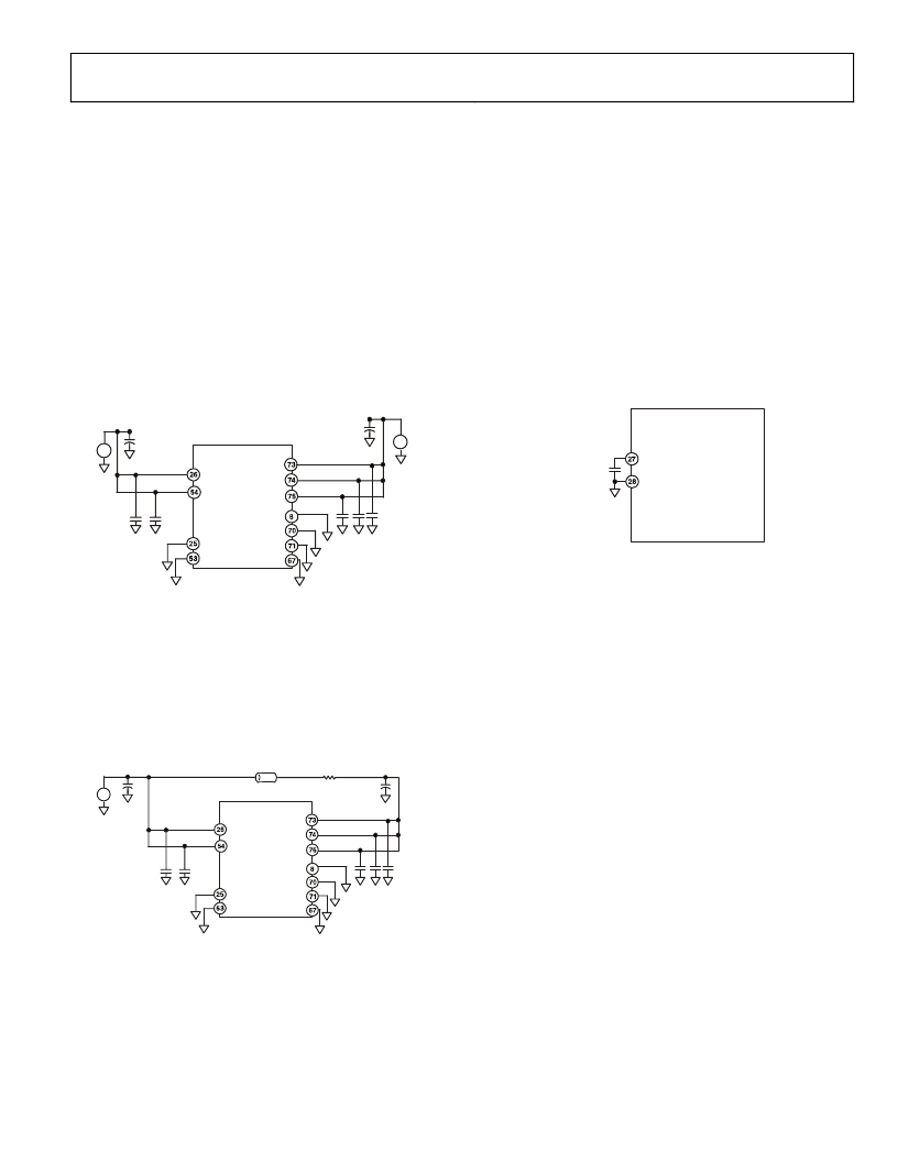
IOV
DD
ADuC7026
AGND
REFGND
AV
DD
-+
0.1
μ
F
10
μ
F
ANALOG SUPPLY
10
μ
F
IOGND
0.1
μ
F
DIGITAL SUPPLY
-+
GND
REF
DACV
DD
DACGND
Figure 38: External dual supply connections
As an alternative to providing two separate power supplies, the
user can help keep AV
DD
quiet by placing a small series resistor
and/or ferrite bead between it and IOV
DD
, and then decoupling
AV
DD
separately to ground. An example of this configuration is
shown in Figure 39. With this configuration other analog
circuitry (such as op amps, voltage reference, and so on) can be
powered from the AV
DD
supply line as well.
IOV
DD
ADuC7026
AGND
REFGND
AV
DD
0.1uF
IOGND
0.1uF
GND
REF
DACV
DD
DACGND
10uF
-
10uF
1.6
V
BEAD
DIGITAL SUPPLY
Figure 39: external single supply connections
Notice that in both Figure 38 and Figure 39, a large value (10
μ
F) reservoir capacitor sits on IOV
DD
and a separate 10
μ
F
capacitor sits on AV
DD
. Also, local small-value (0.1
μ
F)
capacitors are located at each AV
DD
and IOV
DD
pin of the chip.
As per standard design practice, be sure to include all of these
capacitors, and ensure the smaller capacitors are close to each
AV
DD
pin with trace lengths as short as possible. Connect the
ground terminal of each of these capacitors directly to the
underlying ground plane. Finally, it should also be noted that,
at all times, the analog and digital ground pins on the
ADuC702x must be referenced to the same system ground
reference point.
Linear Voltage regulator
The ADuC702x requires a single 3.3V supply but the core logic
requires a 2.5V supply. An on-chip linear regulator generates the
2.5V from IOV
DD
for the core logic. LV
DD
pin 21 is the 2.5V
supply for the core logic. An external compensation capacitor of
0.47
μ
F must be connected between LV
DD
and DGND (as close
as possible to these pins) to act as a tank of charge as shown
Figure 40.
ADuC7026
0.47
μ
F
DGND
LV
DD
Figure 40: voltage regulator connections
The LV
DD
pin should not be used for any other chip. It is also
recommended that the IOV
DD
has excellent power supply
decoupling this to help improving line regulation performance
of the on-chip voltage regulator.
GROUNDING
RECOMMENDATIONS
AND
BOARD
LAYOUT
As with all high resolution data converters, special attention
must be paid to grounding and PC board layout of ADuC702x-
based designs in order to achieve optimum performance from
the ADCs and DAC.
Although the ADuC702x has separate pins for analog and
digital ground (AGND and IOGND), the user must not tie
these to two separate ground planes unless the two ground
planes are connected together very close to the ADuC702x, as
illustrated in the simplified example of Figure 41a. In systems
where digital and analog ground planes are connected together
somewhere else (at the system’s power supply for example),
they cannot be connected again near the ADuC702x since a
ground loop would result. In these cases, tie the ADuC702x’s
AGND and IOGND Pins all to the analog ground plane, as
illustrated in Figure 41b. In systems with only one ground
plane, ensure that the digital and analog components are
physically separated onto separate halves of the board such that
digital return currents do not flow near analog circuitry and
vice versa. The ADuC702x can then be placed between the
相關(guān)PDF資料 |
PDF描述 |
|---|---|
| ADUC7024BST62 | Precision Analog Microcontroller 12-bit Analog I/O, ARM7TDMI MCU |
| ADUC7025BCP32 | Precision Analog Microcontroller 12-bit Analog I/O, ARM7TDMI MCU |
| ADUC7025BCP62 | Precision Analog Microcontroller 12-bit Analog I/O, ARM7TDMI MCU |
| ADUC7026BST62 | Precision Analog Microcontroller 12-bit Analog I/O, ARM7TDMI MCU |
| ADUC7027AST62 | Precision Analog Microcontroller 12-bit Analog I/O, ARM7TDMI MCU |
相關(guān)代理商/技術(shù)參數(shù) |
參數(shù)描述 |
|---|---|
| ADUC7024BCP62-U1 | 制造商:Analog Devices 功能描述:FLASH ARM7+10-CH,12-B ADC &2X12-B DAC IC - Trays |
| ADUC7024BCPZ62 | 功能描述:IC MCU FLSH 62K ANLG I/O 64LFCSP RoHS:是 類(lèi)別:集成電路 (IC) >> 嵌入式 - 微控制器, 系列:MicroConverter® ADuC7xxx 標(biāo)準(zhǔn)包裝:60 系列:PSOC® 3 CY8C38xx 核心處理器:8051 芯體尺寸:8-位 速度:67MHz 連通性:EBI/EMI,I²C,LIN,SPI,UART/USART 外圍設(shè)備:電容感應(yīng),DMA,LCD,POR,PWM,WDT 輸入/輸出數(shù):25 程序存儲(chǔ)器容量:64KB(64K x 8) 程序存儲(chǔ)器類(lèi)型:閃存 EEPROM 大小:2K x 8 RAM 容量:8K x 8 電壓 - 電源 (Vcc/Vdd):1.71 V ~ 5.5 V 數(shù)據(jù)轉(zhuǎn)換器:A/D 2x20b,D/A 4x8b 振蕩器型:內(nèi)部 工作溫度:-40°C ~ 85°C 封裝/外殼:48-VFQFN 裸露焊盤(pán) 包裝:托盤(pán) |
| ADUC7024BCPZ62I | 功能描述:IC MCU 12BIT 1MSPS ANLG 64LFCSP RoHS:是 類(lèi)別:集成電路 (IC) >> 嵌入式 - 微控制器, 系列:MicroConverter® ADuC7xxx 標(biāo)準(zhǔn)包裝:38 系列:Encore!® XP® 核心處理器:eZ8 芯體尺寸:8-位 速度:5MHz 連通性:IrDA,UART/USART 外圍設(shè)備:欠壓檢測(cè)/復(fù)位,LED,POR,PWM,WDT 輸入/輸出數(shù):16 程序存儲(chǔ)器容量:4KB(4K x 8) 程序存儲(chǔ)器類(lèi)型:閃存 EEPROM 大小:- RAM 容量:1K x 8 電壓 - 電源 (Vcc/Vdd):2.7 V ~ 3.6 V 數(shù)據(jù)轉(zhuǎn)換器:- 振蕩器型:內(nèi)部 工作溫度:-40°C ~ 105°C 封裝/外殼:20-SOIC(0.295",7.50mm 寬) 包裝:管件 其它名稱(chēng):269-4116Z8F0413SH005EG-ND |
| ADUC7024BCPZ62I-RL | 功能描述:IC MCU 12BIT 1MSPS ANLG 64LFCSP RoHS:是 類(lèi)別:集成電路 (IC) >> 嵌入式 - 微控制器, 系列:MicroConverter® ADuC7xxx 標(biāo)準(zhǔn)包裝:38 系列:Encore!® XP® 核心處理器:eZ8 芯體尺寸:8-位 速度:5MHz 連通性:IrDA,UART/USART 外圍設(shè)備:欠壓檢測(cè)/復(fù)位,LED,POR,PWM,WDT 輸入/輸出數(shù):16 程序存儲(chǔ)器容量:4KB(4K x 8) 程序存儲(chǔ)器類(lèi)型:閃存 EEPROM 大小:- RAM 容量:1K x 8 電壓 - 電源 (Vcc/Vdd):2.7 V ~ 3.6 V 數(shù)據(jù)轉(zhuǎn)換器:- 振蕩器型:內(nèi)部 工作溫度:-40°C ~ 105°C 封裝/外殼:20-SOIC(0.295",7.50mm 寬) 包裝:管件 其它名稱(chēng):269-4116Z8F0413SH005EG-ND |
| ADUC7024BCPZ62-RL | 制造商:Analog Devices 功能描述:MCU 16-bit/32-bit ADuC7xxx ARM7TDMI RISC 62KB Flash 3.3V 64-Pin LFCSP EP T/R |
發(fā)布緊急采購(gòu),3分鐘左右您將得到回復(fù)。