- 您現在的位置:買賣IC網 > PDF目錄374039 > ADUC814ARU-REEL7 (ANALOG DEVICES INC) Circular Connector; MIL SPEC:MIL-DTL-38999 Series I; Body Material:Metal; Series:LJT; No. of Contacts:37; Connector Shell Size:25; Connecting Termination:Crimp; Circular Shell Style:Jam Nut Receptacle; Body Style:Straight RoHS Compliant: No PDF資料下載
參數資料
| 型號: | ADUC814ARU-REEL7 |
| 廠商: | ANALOG DEVICES INC |
| 元件分類: | 微控制器/微處理器 |
| 英文描述: | Circular Connector; MIL SPEC:MIL-DTL-38999 Series I; Body Material:Metal; Series:LJT; No. of Contacts:37; Connector Shell Size:25; Connecting Termination:Crimp; Circular Shell Style:Jam Nut Receptacle; Body Style:Straight RoHS Compliant: No |
| 中文描述: | 8-BIT, FLASH, 16.78 MHz, MICROCONTROLLER, PDSO28 |
| 封裝: | 4.40 X 9.70 MM, MO-153AE, TSSOP-28 |
| 文件頁數: | 60/72頁 |
| 文件大小: | 846K |
| 代理商: | ADUC814ARU-REEL7 |
第1頁第2頁第3頁第4頁第5頁第6頁第7頁第8頁第9頁第10頁第11頁第12頁第13頁第14頁第15頁第16頁第17頁第18頁第19頁第20頁第21頁第22頁第23頁第24頁第25頁第26頁第27頁第28頁第29頁第30頁第31頁第32頁第33頁第34頁第35頁第36頁第37頁第38頁第39頁第40頁第41頁第42頁第43頁第44頁第45頁第46頁第47頁第48頁第49頁第50頁第51頁第52頁第53頁第54頁第55頁第56頁第57頁第58頁第59頁當前第60頁第61頁第62頁第63頁第64頁第65頁第66頁第67頁第68頁第69頁第70頁第71頁第72頁
ADuC814
ADuC814 HARDWARE DESIGN CONSIDERATIONS
This section outlines some key hardware design considerations
for integrating the ADuC814 into any hardware system.
Rev. A | Page 60 of 72
CLOCK OSCILLATOR
As described earlier, the core clock frequency for the ADuC814
is generated from an on-chip PLL that locks onto a multiple
(512 times) of 32.768 kHz. The latter is generated from an
internal clock oscillator. To use the internal clock oscillator,
connect a 32.768 kHz parallel resonant crystal between XTAL1
and XTAL2 pins (Pins 26 and 27) as shown in Figure 54.
As shown in the typical external crystal connection diagram in
Figure 54, two internal 12 pF capacitors are provided on-chip.
These are connected internally, directly to the XTAL1 and
XTAL2 pins. The total input capacitances at both pins is
detailed in the Specifications table. The value of the total load
capacitance required for the external crystal should be the value
recommended by the crystal manufacturer for use with that
specific crystal. In many cases, because of the on-chip capacitors,
additional external load capacitors are not required.
ADuC814
TO PLL
12pF
12pF
XTAL1
XTAL2
0
Figure 54. External Parallel Resonant Crystal Connections
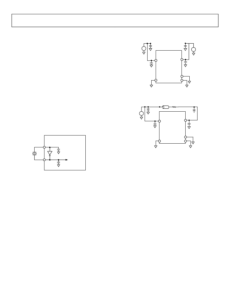
As an alternative to providing two separate power supplies,
AV
DD
can be kept quiet by placing a small series resistor and/or
ferrite bead between it and DV
DD
, and then decoupling AV
DD
separately to ground. An example of this configuration is shown
in Figure 56. With this configuration, other analog circuitry
(such as op amps and voltage reference) can be powered from
the AV
DD
supply line as well.
POWER SUPPLIES
The ADuC814’s operational power supply voltage range is 2.7 V
to 5.5 V. Although the guaranteed data sheet specifications are
given only for power supplies within 2.7 V to 3.3 V or 4.5 V to
5.5 V, (±10% of the nominal level), the chip can function equally
well at any power supply level between 2.7 V and 5.5 V.
Users should separate analog and digital power supply pins
(AV
DD
and DV
DD
) and allow AV
DD
to be kept relatively free of
noisy digital signals often present on the system DV
DD
line. In
this mode, the part can also operate with split supplies as long
as the supply voltages are within 0.3 V of each other. A typical
split-supply configuration is show in Figure 55.
DV
DD
AGND
AV
DD
–
+
0.1
μ
F
10
μ
F
ANALOG SUPPLY
10
μ
F
DGND
0.1
μ
F
DIGITAL SUPPLY
–
+
ADuC814
0
Figure 55. External Dual-Supply Connections
DV
DD
AGND
AV
DD
DGND
DIGITAL SUPPLY
–
+
BEAD
1.6
0.1
μ
F
0.1
μ
F
10
μ
F
10
μ
F
ADuC814
0
Figure 56. External Single-Supply Connections
Notice that in both Figure 55 and Figure 56, a large value
(10 μF) reservoir capacitor sits on DV
DD
and a separate 10 μF
capacitor sits on AVDD. Also, local small-value (0.1 μF) capacitors
are located at each V
DD
pin of the chip. As per standard design
practice, be sure to include all of these capacitors, and ensure
that the smaller capacitors are closest to each AV
DD
pin with
trace lengths as short as possible. Connect the ground terminal
of each of these capacitors directly to the underlying ground
plane. Finally, note that, at all times, the analog and digital ground
pins on the ADuC814 should be referenced to the same system
ground reference point.
POWER CONSUMPTION
The CORE values given represent the current drawn by DV
DD
,
while the rest (ADC and DAC) are pulled by the AV
DD
pin and
can be disabled in software when not in use. The other on-chip
peripherals (such as watchdog timer and power supply monitor)
consume negligible current and are therefore lumped in with
the CORE operating current here. Of course, the user must add
any currents sourced by the parallel and serial I/O pins, and that
sourced by the DAC, in order to determine the total current
needed at the ADuC814’s supply pins. Also, current drawn from
the DVDD supply increases by approximately 5 mA during the
Flash/EE erase and program cycles.
相關PDF資料 |
PDF描述 |
|---|---|
| ADUC814BRU | Circular Connector; MIL SPEC:MIL-DTL-38999 Series I; Body Material:Metal; Series:LJT; No. of Contacts:37; Connector Shell Size:25; Connecting Termination:Crimp; Circular Shell Style:Jam Nut Receptacle; Body Style:Straight RoHS Compliant: No |
| ADUC814BRU-REEL | Circular Connector; No. of Contacts:56; Series:LJT07R; Body Material:Aluminum; Connecting Termination:Crimp; Connector Shell Size:25; Circular Contact Gender:Pin; Circular Shell Style:Jam Nut Receptacle; Insert Arrangement:25-4 |
| ADUC814BRU-REEL7 | Circular Connector; No. of Contacts:61; Series:LJT07R; Body Material:Aluminum; Connecting Termination:Crimp; Connector Shell Size:25; Circular Contact Gender:Pin; Circular Shell Style:Jam Nut Receptacle; Insert Arrangement:25-61 |
| ADUC814 | MicroConverter, Small Package 12-Bit ADC with Embedded Flash MCU |
| ADUC814ARU | MicroConverter, Small Package 12-Bit ADC with Embedded Flash MCU |
相關代理商/技術參數 |
參數描述 |
|---|---|
| ADUC814ARUZ | 功能描述:IC ADC 12BIT W/FLASH MCU 28TSSOP RoHS:是 類別:集成電路 (IC) >> 嵌入式 - 微控制器, 系列:MicroConverter® ADuC8xx 產品培訓模塊:MCU Product Line Introduction XMEGA Introduction AVR XMEGA USB Connectivity 標準包裝:90 系列:AVR® XMEGA 核心處理器:AVR 芯體尺寸:8/16-位 速度:32MHz 連通性:I²C,IrDA,SPI,UART/USART 外圍設備:欠壓檢測/復位,DMA,POR,PWM,WDT 輸入/輸出數:50 程序存儲器容量:192KB(96K x 16) 程序存儲器類型:閃存 EEPROM 大小:4K x 8 RAM 容量:16K x 8 電壓 - 電源 (Vcc/Vdd):1.6 V ~ 3.6 V 數據轉換器:A/D 16x12b; D/A 2x12b 振蕩器型:內部 工作溫度:-40°C ~ 85°C 封裝/外殼:64-TQFP 包裝:托盤 配用:ATSTK600-RC14-ND - STK600 SOCKET/ADAPTER 64TQFPATSTK600-TQFP64-ND - STK600 SOCKET/ADAPTER 64-TQFPATAVRONEKIT-ND - KIT AVR/AVR32 DEBUGGER/PROGRMMRATAVRISP2-ND - PROGRAMMER AVR IN SYSTEM |
| ADUC814ARUZ-REEL | 功能描述:IC MCU FLASH 12BIT ADC 28TSSOP RoHS:是 類別:集成電路 (IC) >> 嵌入式 - 微控制器, 系列:MicroConverter® ADuC8xx 標準包裝:38 系列:Encore!® XP® 核心處理器:eZ8 芯體尺寸:8-位 速度:5MHz 連通性:IrDA,UART/USART 外圍設備:欠壓檢測/復位,LED,POR,PWM,WDT 輸入/輸出數:16 程序存儲器容量:4KB(4K x 8) 程序存儲器類型:閃存 EEPROM 大小:- RAM 容量:1K x 8 電壓 - 電源 (Vcc/Vdd):2.7 V ~ 3.6 V 數據轉換器:- 振蕩器型:內部 工作溫度:-40°C ~ 105°C 封裝/外殼:20-SOIC(0.295",7.50mm 寬) 包裝:管件 其它名稱:269-4116Z8F0413SH005EG-ND |
| ADUC814ARUZ-REEL7 | 功能描述:IC MCU FLASH 12BIT ADC 28TSSOP RoHS:是 類別:集成電路 (IC) >> 嵌入式 - 微控制器, 系列:MicroConverter® ADuC8xx 標準包裝:38 系列:Encore!® XP® 核心處理器:eZ8 芯體尺寸:8-位 速度:5MHz 連通性:IrDA,UART/USART 外圍設備:欠壓檢測/復位,LED,POR,PWM,WDT 輸入/輸出數:16 程序存儲器容量:4KB(4K x 8) 程序存儲器類型:閃存 EEPROM 大小:- RAM 容量:1K x 8 電壓 - 電源 (Vcc/Vdd):2.7 V ~ 3.6 V 數據轉換器:- 振蕩器型:內部 工作溫度:-40°C ~ 105°C 封裝/外殼:20-SOIC(0.295",7.50mm 寬) 包裝:管件 其它名稱:269-4116Z8F0413SH005EG-ND |
| ADUC814BRU | 功能描述:IC ADC 12BIT W/FLASH MCU 28TSSOP RoHS:否 類別:集成電路 (IC) >> 嵌入式 - 微控制器, 系列:MicroConverter® ADuC8xx 標準包裝:38 系列:Encore!® XP® 核心處理器:eZ8 芯體尺寸:8-位 速度:5MHz 連通性:IrDA,UART/USART 外圍設備:欠壓檢測/復位,LED,POR,PWM,WDT 輸入/輸出數:16 程序存儲器容量:4KB(4K x 8) 程序存儲器類型:閃存 EEPROM 大小:- RAM 容量:1K x 8 電壓 - 電源 (Vcc/Vdd):2.7 V ~ 3.6 V 數據轉換器:- 振蕩器型:內部 工作溫度:-40°C ~ 105°C 封裝/外殼:20-SOIC(0.295",7.50mm 寬) 包裝:管件 其它名稱:269-4116Z8F0413SH005EG-ND |
| ADUC814BRU-REEL | 制造商:Analog Devices 功能描述:MCU 8-bit ADuC8xx 8052 CISC 8KB Flash 3V/5V 28-Pin TSSOP T/R 制造商:Analog Devices 功能描述:MCU 8BIT CISC 8KB FLASH 3.3V/5V 28TSSOP - Tape and Reel 制造商:Analog Devices Inc. 功能描述:8-bit Microcontrollers - MCU 12 BIT ADC WITH EMBEDDED 8-BIT MICRO I.C |
發布緊急采購,3分鐘左右您將得到回復。