- 您現在的位置:買賣IC網 > PDF目錄374042 > ADUM1401CRWZ (ANALOG DEVICES INC) Quad-Channel Digital Isolators PDF資料下載
參數資料
| 型號: | ADUM1401CRWZ |
| 廠商: | ANALOG DEVICES INC |
| 元件分類: | 模擬信號調理 |
| 英文描述: | Quad-Channel Digital Isolators |
| 中文描述: | SPECIALTY ANALOG CIRCUIT, PDSO16 |
| 封裝: | ROHS COMPLIANT, MS-013AA, SOIC-16 |
| 文件頁數: | 19/24頁 |
| 文件大小: | 797K |
| 代理商: | ADUM1401CRWZ |
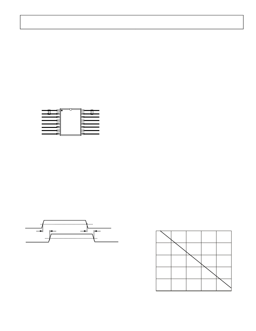
ADuM1400/ADuM1401/ADuM1402
APPLICATION INFORMATION
PC BOARD LAYOUT
The ADuM140x digital isolator requires no external interface
circuitry for the logic interfaces. Power supply bypassing is
strongly recommended at the input and output supply pins
(Figure 17). Bypass capacitors are most conveniently connected
between Pins 1 and 2 for V
DD1
and between Pins 15 and 16 for
V
DD2
. The capacitor value should be between 0.01 μF and 0.1 μF.
The total lead length between both ends of the capacitor and
the input power supply pin should not exceed 20 mm. Bypass-
ing between Pins 1 and 8 and between Pins 9 and 16 should also
be considered unless the ground pair on each package side is
connected close to the package.
Rev. B | Page 19 of 24
V
GND
1
V
IA
V
IB
V
IC/OC
V
ID/OD
E1
GND
1
V
GND
2
V
OA
V
OB
V
OC/IC
V
OD/ID
V
E2
GND
2
0
Figure 17. Recommended Printed Circuit Board Layout
In applications involving high common-mode transients, care
should be taken to ensure that board coupling across the isola-
tion barrier is minimized. Furthermore, the board layout should
be designed such that any coupling that does occur equally
affects all pins on a given component side. Failure to ensure this
could cause voltage differentials between pins exceeding the
device’s Absolute Maximum Ratings, thereby leading to latch-up
or permanent damage.
PROPAGATION DELAY-RELATED PARAMETERS
Propagation delay is a parameter that describes the time it takes
a logic signal to propagate through a component. The propaga-
tion delay to a logic low output may differ from the propagation
delay to a logic high.
INPUT (V
IX
)
OUTPUT (V
OX
)
t
PLH
t
PHL
50%
50%
0
Figure 18. Propagation Delay Parameters
Pulse-width distortion is the maximum difference between
these two propagation delay values and is an indication of how
accurately the input signal’s timing is preserved.
Channel-to-channel matching refers to the maximum that
amount the propagation delay differs between channels within a
single ADuM140x component.
Propagation delay skew refers to the maximum that amount the
propagation delay differs between multiple ADuM140x compo-
nents operating under the same conditions.
DC CORRECTNESS AND MAGNETIC FIELD IMMUNITY
Positive and negative logic transitions at the isolator input
cause narrow (~1 ns) pulses to be sent to the decoder via the
transformer. The decoder is bistable and is, therefore, either set
or reset by the pulses, indicating input logic transitions. In the
absence of logic transitions at the input for more than 2 μs, a
periodic set of refresh pulses indicative of the correct input state
are sent to ensure dc correctness at the output. If the decoder
receives no internal pulses of more than about 5 μs, the input
side is assumed to be unpowered or nonfunctional, in which
case the isolator output is forced to a default state (see Table 10)
by the watchdog timer circuit.
The limitation on the ADuM140x’s magnetic field immunity is
set by the condition in which induced voltage in the transformer’s
receiving coil is sufficiently large to either falsely set or reset the
decoder. The following analysis defines the conditions under
which this may occur. The 3 V operating condition of the
ADuM140x is examined because it represents the most
susceptible mode of operation.
The pulses at the transformer output have an amplitude greater than
1.0 V The decoder has a sensing threshold at about 0.5 V therefore
establishing a 0.5 V margin in which induced voltages can be toler-
ated. The voltage induced across the receiving coil is given by
V
= (
–d
β
/dt
)
∑
∏
r
n2
;
n
= 1, 2,…,
N
where:
β is magnetic flux density (gauss).
N
is the number of turns in the receiving coil.
r
n
is the radius of the n
th
turn in the receiving coil (cm).
Given the geometry of the receiving coil in the ADuM140x and
an imposed requirement that the induced voltage be at most
50% of the 0.5 V margin at the decoder, a maximum allowable
magnetic field is calculated as shown in Figure 19.
MAGNETIC FIELD FREQUENCY (Hz)
100.000
M
D
0.001
1M
10.000
0.010
1k
10k
10M
0.100
1.000
100M
100k
0
Figure 19. Maximum Allowable External Magnetic Flux Density
相關PDF資料 |
PDF描述 |
|---|---|
| ADUM1402ARW | Quad-Channel Digital Isolators |
| ADUM1402ARWZ | Quad-Channel Digital Isolators |
| ADUM1402BRW | Quad-Channel Digital Isolators |
| ADUM1402CRW | Quad-Channel Digital Isolators |
| ADUM1402BRWZ | Quad-Channel Digital Isolators |
相關代理商/技術參數 |
參數描述 |
|---|---|
| ADUM1401CRWZ-RL | 功能描述:IC DGITAL ISOLATOR 4CH 16-SOIC RoHS:是 類別:隔離器 >> 數字隔離器 系列:iCoupler® 標準包裝:66 系列:iCoupler® 輸入 - 1 側/2 側:2/2 通道數:4 電源電壓:3.3V,5V 電壓 - 隔離:2500Vrms 數據速率:25Mbps 傳輸延遲:60ns 輸出類型:邏輯 封裝/外殼:20-SSOP(0.209",5.30mm 寬) 供應商設備封裝:20-SSOP 包裝:管件 工作溫度:-40°C ~ 105°C |
| ADUM1401WRWZ | 制造商:Analog Devices 功能描述: |
| ADUM1401WRWZ-RL | 制造商:Analog Devices 功能描述: |
| ADUM1401WSRWZ | 功能描述:IC ISOLATOR DIG 4CH 125C 16SOIC RoHS:是 類別:隔離器 >> 數字隔離器 系列:iCoupler® 標準包裝:66 系列:iCoupler® 輸入 - 1 側/2 側:2/2 通道數:4 電源電壓:3.3V,5V 電壓 - 隔離:2500Vrms 數據速率:25Mbps 傳輸延遲:60ns 輸出類型:邏輯 封裝/外殼:20-SSOP(0.209",5.30mm 寬) 供應商設備封裝:20-SSOP 包裝:管件 工作溫度:-40°C ~ 105°C |
| ADUM1401WSRWZ33 | 功能描述:IC DGTL ISO 4CH LOGIC 16SOIC 制造商:analog devices inc. 系列:* 零件狀態:上次購買時間 標準包裝:47 |
發布緊急采購,3分鐘左右您將得到回復。