- 您現在的位置:買賣IC網 > PDF目錄374047 > ADV7185KST (ANALOG DEVICES INC) Professional NTSC/PAL Video Decoder with 10-Bit CCIR656 Output PDF資料下載
參數資料
| 型號: | ADV7185KST |
| 廠商: | ANALOG DEVICES INC |
| 元件分類: | 顏色信號轉換 |
| 英文描述: | Professional NTSC/PAL Video Decoder with 10-Bit CCIR656 Output |
| 中文描述: | COLOR SIGNAL DECODER, PQFP80 |
| 封裝: | PLASTIC, LQFP-80 |
| 文件頁數: | 18/41頁 |
| 文件大小: | 730K |
| 代理商: | ADV7185KST |
第1頁第2頁第3頁第4頁第5頁第6頁第7頁第8頁第9頁第10頁第11頁第12頁第13頁第14頁第15頁第16頁第17頁當前第18頁第19頁第20頁第21頁第22頁第23頁第24頁第25頁第26頁第27頁第28頁第29頁第30頁第31頁第32頁第33頁第34頁第35頁第36頁第37頁第38頁第39頁第40頁第41頁
REV. 0
–18–
ADV7185
Manual Clock Control
The ADV7185 offers several output clock mode options: the
output clock frequency can be set by the input video line length, a
fixed 27 MHz output, or by a user-programmable value. Informa-
tion on the clock control register at 28h can be found in the
register access map. When Bit 6 of this register (CLKMANE) is
set to Logic “1,” the output clock frequency will be determined
by
the user-programmable value (CLKVAL[15:0]). Using this
mode,
the output clock frequency is calculated as:
LLC
CLKVAL
MHz
=
×
×
×
[
17: ]
2
28
3
16
27
20
For example, a required clock frequency of 25 MHz would yield
a CLKVAL of 2D266h (184934).
Color Subcarrier Control
The color subcarrier manual frequency control register
(CSMF[27:0]) can be used to set the DDFS block to a user-
defined frequency. This function can be useful if the color
subcarrier frequency of the incoming video signal is outside
the standard F
SC
lock range. Setting Bit 4 reg 23h (CSM) to a
Logic “1” enables the manual frequency control, the frequency
of which will be determined by CSMF[27:0]. The value of
CSMF[27:0] can be calculated as:
CSMF
F
MHz
SC
[
2: ]
2
27
28
=
×
*
*
Required
MPU PORT DESCRIPTION
The ADV7185 supports a 2-wire serial (I
2
C-compatible) micro-
processor bus driving multiple peripherals. Two inputs, serial
data (SDATA) and serial clock (SCLOCK), carry information
between any device connected to the bus. Each slave device is
recognized by a unique address. The ADV7185 has two possible
slave addresses for both read and write operations. These are
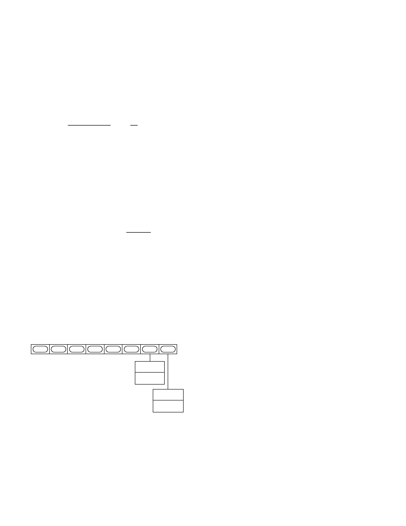
unique addresses for the device and are illustrated in Figure 27.
The LSB sets either a read or write operation. Logic Level “1”
corresponds to a read operation while Logic Level “0” corre-
sponds to a write operation. A1 is set by setting the ALSB pin of
the ADV7185 to Logic Level “0” or Logic Level “1.”
1
0
0
0
1
0
A1
X
ADDRESS
CONTROL
SET UP BY
ALSB
READ/WRITE
CONTROL
0 WRITE
1 READ
Figure 27. Slave Address
To control the device on the bus the following protocol must
be followed. First the master initiates a data transfer by estab-
lishing a start condition, defined by a high to low transition on
SDATA while SCLOCK remains high. This indicates that an
address/data stream will follow. All peripherals respond to the
start condition and shift the next 8 bits (7-Bit Address + R/
W
Bit). The bits are transferred from MSB down to LSB. The
peripheral that recognizes the transmitted address responds by
pulling the data line low during the ninth clock pulse. This is
known as an acknowledge bit. All other devices withdraw
from the bus at this point and maintain an idle condition. The
idle condition is where the device monitors the SDATA and
SCLOCK lines waiting for the start condition and the correct
transmitted address. The R/
W
bit determines the direction of
the data. A Logic “0” on the LSB of the first byte means that
the master will write information to the peripheral. A Logic “1”
on the LSB of the first byte means that the master will read
information from the peripheral.
The ADV7185 acts as a standard slave device on the bus. The
data on the SDATA pin is 8 bits long, supporting the 7-bit
addresses plus the R/
W
bit. The ADV7185 has 71 subaddresses
to enable access to the internal registers. It therefore interprets
the first byte as the device address and the second byte as the
starting subaddress. The subaddresses autoincrement, allowing
data to be written to or read from the starting subaddress. A
data transfer is always terminated by a stop condition. The user
can also access any unique subaddress register on a one-by-one
basis, without having to update all the registers.
Stop and start conditions can be detected at any stage during
the data transfer. If these conditions are asserted out of sequence
with normal read and write operations, they cause an immediate
jump to the idle condition. During a given SCLOCK high
period, the user should only issue one start condition, one stop
condition, or a single stop condition followed by a single start
condition. If an invalid subaddress is issued by the user, the
ADV7185 will not issue an acknowledge and will return to the
idle condition. If the user exceeds the highest subaddress in
autoincrement mode, the following action will be taken:
1. In read mode, the highest subaddress register contents
will continue to be output until the master device issues
a no-acknowledge. This indicates the end of a read. A
no-acknowledge condition is where the SDATA line is
not pulled low on the ninth pulse.
2. In write mode, the data for the invalid byte will not be loaded
into any subaddress register, a no-acknowledge will be issued
by the ADV7185, and the part will return to the idle condition.
相關PDF資料 |
PDF描述 |
|---|---|
| ADV7190KST | Video Encoder with Six 10-Bit DACs and Video Encoder with Six DAC Outputs |
| ADV7191 | Video Encoder with Six 10-Bit DACs and Video Encoder with Six DAC Outputs |
| ADV7191KST | Video Encoder with Six 10-Bit DACs and Video Encoder with Six DAC Outputs |
| ADV7190 | Video Encoder with Six 10-Bit DACs and Video Encoder with Six DAC Outputs |
| ADV7192KST | Video Encoder with Six 10-Bit DACs, 54 MHz Oversampling and Progressive Scan Inputs |
相關代理商/技術參數 |
參數描述 |
|---|---|
| ADV7186 | 制造商:AD 制造商全稱:Analog Devices 功能描述:Video Decoder and Display Processor |
| ADV7186BBCZ | 功能描述:IC VIDEO DECODER 196CSPBGA RoHS:是 類別:集成電路 (IC) >> 線性 - 視頻處理 系列:- 產品變化通告:Product Discontinuation 07/Mar/2011 標準包裝:3,000 系列:OMNITUNE™ 類型:調諧器 應用:移動電話,手機,視頻顯示器 安裝類型:表面貼裝 封裝/外殼:65-WFBGA 供應商設備封裝:PG-WFSGA-65 包裝:帶卷 (TR) 其它名稱:SP000365064 |
| ADV7186BBCZ-RL | 功能描述:IC VIDEO DECODER 196CSPBGA RoHS:是 類別:集成電路 (IC) >> 線性 - 視頻處理 系列:- 產品變化通告:Product Discontinuation 07/Mar/2011 標準包裝:3,000 系列:OMNITUNE™ 類型:調諧器 應用:移動電話,手機,視頻顯示器 安裝類型:表面貼裝 封裝/外殼:65-WFBGA 供應商設備封裝:PG-WFSGA-65 包裝:帶卷 (TR) 其它名稱:SP000365064 |
| ADV7186BBCZ-T | 功能描述:IC VIDEO DECODER 196CSPBGA RoHS:是 類別:集成電路 (IC) >> 線性 - 視頻處理 系列:- 產品變化通告:Product Discontinuation 07/Mar/2011 標準包裝:3,000 系列:OMNITUNE™ 類型:調諧器 應用:移動電話,手機,視頻顯示器 安裝類型:表面貼裝 封裝/外殼:65-WFBGA 供應商設備封裝:PG-WFSGA-65 包裝:帶卷 (TR) 其它名稱:SP000365064 |
| ADV7186BBCZ-TL | 功能描述:IC VIDEO DECODER 196CSPBGA RoHS:是 類別:集成電路 (IC) >> 線性 - 視頻處理 系列:- 產品變化通告:Product Discontinuation 07/Mar/2011 標準包裝:3,000 系列:OMNITUNE™ 類型:調諧器 應用:移動電話,手機,視頻顯示器 安裝類型:表面貼裝 封裝/外殼:65-WFBGA 供應商設備封裝:PG-WFSGA-65 包裝:帶卷 (TR) 其它名稱:SP000365064 |
發布緊急采購,3分鐘左右您將得到回復。