- 您現在的位置:買賣IC網 > PDF目錄374047 > ADV7340BSTZ (ANALOG DEVICES INC) Multiformat Video Encoder, Six 12-Bit Noise Shaped Video㈢ DACS PDF資料下載
參數資料
| 型號: | ADV7340BSTZ |
| 廠商: | ANALOG DEVICES INC |
| 元件分類: | DAC |
| 英文描述: | Multiformat Video Encoder, Six 12-Bit Noise Shaped Video㈢ DACS |
| 中文描述: | SERIAL INPUT LOADING, 12-BIT DAC, PQFP64 |
| 封裝: | ROHS COMPLIANT, MS-026BCD, LQFP-64 |
| 文件頁數: | 46/88頁 |
| 文件大小: | 1066K |
| 代理商: | ADV7340BSTZ |
第1頁第2頁第3頁第4頁第5頁第6頁第7頁第8頁第9頁第10頁第11頁第12頁第13頁第14頁第15頁第16頁第17頁第18頁第19頁第20頁第21頁第22頁第23頁第24頁第25頁第26頁第27頁第28頁第29頁第30頁第31頁第32頁第33頁第34頁第35頁第36頁第37頁第38頁第39頁第40頁第41頁第42頁第43頁第44頁第45頁當前第46頁第47頁第48頁第49頁第50頁第51頁第52頁第53頁第54頁第55頁第56頁第57頁第58頁第59頁第60頁第61頁第62頁第63頁第64頁第65頁第66頁第67頁第68頁第69頁第70頁第71頁第72頁第73頁第74頁第75頁第76頁第77頁第78頁第79頁第80頁第81頁第82頁第83頁第84頁第85頁第86頁第87頁第88頁
ADV7340/ADV7341
ENHANCED DEFINITION/HIGH DEFINITION ONLY
Subaddress 0x01, Bits[6:4] = 001 or 010
Enhanced definition (ED) or high definition (HD) YCrCb data
can be input in either 4:2:2 or 4:4:4 formats. If desired, dual data
rate (DDR) pixel data inputs can be employed (4:2:2 format only).
Enhanced definition (ED) or high definition (HD) RGB data
can be input in 4:4:4 format (single data rate only).
The clock signal must be provided on the CLKIN_A pin. Input
synchronization signals are provided on the P_HSYNC,
P_VSYNC and P_BLANK pins.
16-/20-Bit 4:2:2 YCrCb Mode (SDR)
Subaddress 0x35, Bit 1 = 0; Subaddress 0x33, Bit 6 = 1
In 16-/20-bit 4:2:2 YCrCb input mode, the Y pixel data is
input on Pin Y9 to Pin Y2/Y0, with Y0 being the LSB in
20-bit input mode.
The CrCb pixel data is input on Pin C9 to Pin C2/C0, with C0
being the LSB in 20-bit input mode.
8-/10-Bit 4:2:2 YCrCb Mode (DDR)
Subaddress 0x35, Bit 1 = 0; Subaddress 0x33, Bit 6 = 1
In 8-/10-bit DDR 4:2:2 YCrCb input mode, the Y pixel data is
input on Pin Y9 to Pin Y2/Y0 upon either the rising or falling
edge of CLKIN_A. Y0 is the LSB in 10-bit input mode.
The CrCb pixel data is also input on Pin Y9 to Pin Y2/Y0
upon the opposite edge of CLKIN_A. Y0 is the LSB in 10-bit
input mode.
Whether the Y data is clocked in upon the rising or falling edge
of CLKIN_A is determined by Subaddress 0x01, Bits[2:1] (see
Figure 52 and Figure 53).
Rev. 0 | Page 46 of 88
3FF
00
00
X
Y
Y0
Y1
Cr0
CLKIN_A
NOTES
1. SUBADDRESS 0x01 [2:1] SHOULD BE SET TO 00 IN THIS CASE.
Y[9:Y]
Cb0
0
Figure 52. ED/HD-DDR Input Sequence (EAV/SAV)—Option A
3FF
00
00
XY
Cb0
Cr0
Y1
CLKIN_
A
Y[9:0]
Y0
NOTES
1. SUBADDRESS 0x01 [2:1] SHOULD BE SET TO 11 IN THIS CASE.
0
Figure 53. ED/HD-DDR Input Sequence (EAV/SAV)—Option B
24-/30-Bit 4:4:4 YCrCb Mode
Subaddress 0x35, Bit 1 = 0; Subaddress 0x33, Bit 6 = 0
In 24-/30-bit 4:4:4 YCrCb input mode, the Y pixel data is input on
Pin Y9 to Pin Y2/Y0, with Y0 being the LSB in 30-bit input mode.
The Cr pixel data is input on Pin S9 to Pin S2/S0, with S0 being
the LSB in 30-bit input mode.
The Cb pixel data is input on Pin C9 to Pin C2/C0, with C0
being the LSB in 30-bit input mode.
24-/30-Bit 4:4:4 RGB Mode
Subaddress 0x35, Bit 1 = 1
In 24-/30-bit 4:4:4 RGB input mode, the red pixel data is input
on Pin S9 to Pin S2/S0, the green pixel data is input on Pin Y9
to Pin Y2/Y0, and the blue pixel data is input on Pin C9 to
Pin C2/C0. S0, Y0, and C0 are the respective bus LSBs in 30-bit
input mode.
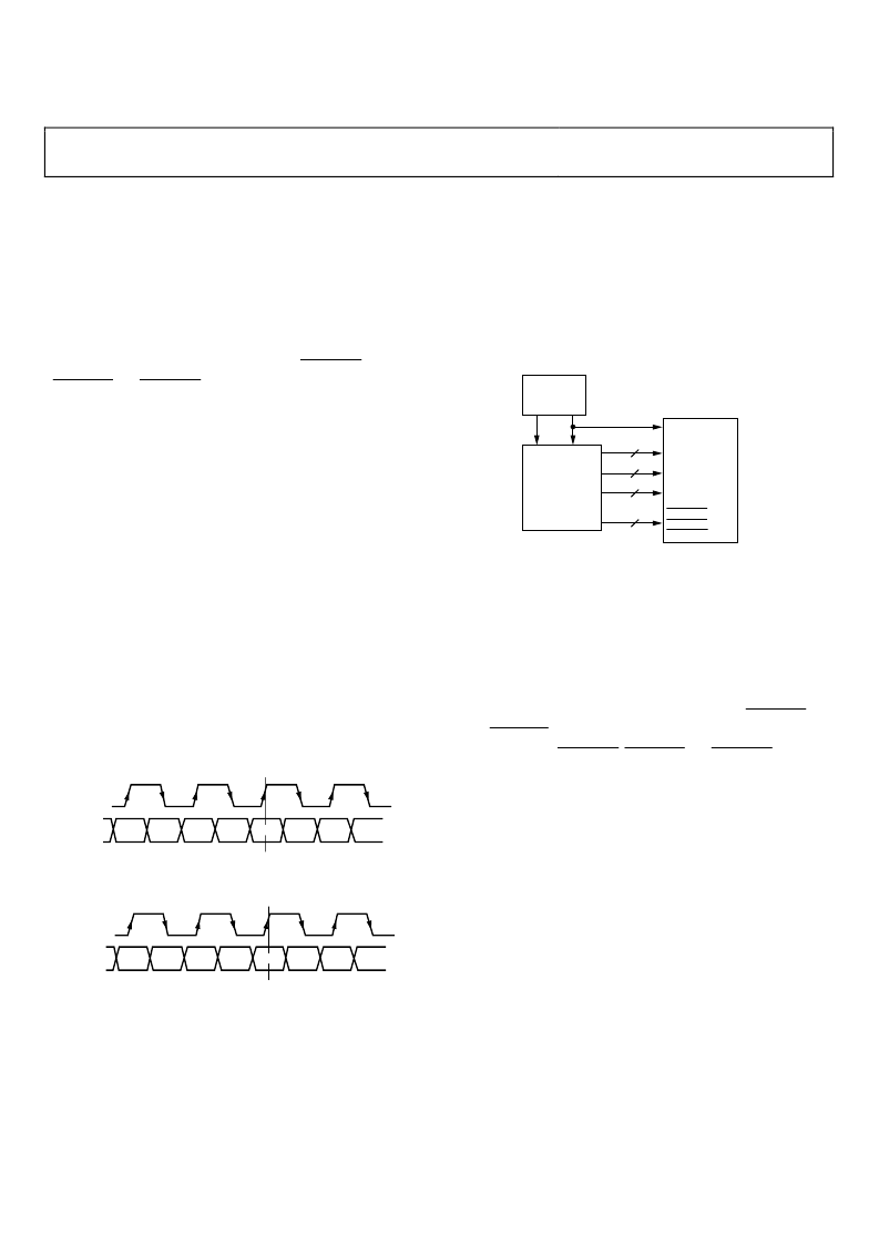
MPEG2
DECODER
CLKIN_
A
C[9:0]
S[9:0]
Y[9:0]
INTERLACED TO
PROGRESSIVE
YCrCb
ADV7340/
ADV7341
P_VSYNC,
P_HSYNC,
P_BLANK
10
Cb
10
Cr
10
Y
3
0
Figure 54. ED/HD Only Example Application
SIMULTANEOUS STANDARD DEFINITION AND
ENHANCED DEFINITION/HIGH DEFINITION
Subaddress 0x01, Bits[6:4] = 011 or 100
The ADV7340/ADV7341 are able to simultaneously process SD
4:2:2 YCrCb data and ED/HD 4:2:2 YCrCb data. The 27 MHz
SD clock signal must be provided on the CLKIN_A pin. The
ED/HD clock signal must be provided on the CLKIN_B pin. SD
input synchronization signals are provided on the S_HSYNC
and S_VSYNC pins. ED/HD input synchronization signals are
provided on the P_HSYNC, P_VSYNC and P_BLANK pins.
SD 8-/10-Bit 4:2:2 YCrCb and ED/HD-SDR 16-/20-Bit
4:2:2 YCrCb
The SD 8-/10-bit 4:2:2 YCrCb pixel data is input on Pin S9 to
Pin S2/S0, with S0 being the LSB in 10-bit input mode.
The ED/HD 16-/20-bit 4:2:2 Y pixel data is input on Pin Y9 to
Pin Y2/Y0, with Y0 being the LSB in 20-bit input mode.
The ED/HD 16-/20-bit 4:2:2 CrCb pixel data is input on Pin C9
to Pin C2/C0, with C0 being the LSB in 20-bit input mode.
SD 8-/10-Bit 4:2:2 YCrCb and ED/HD-DDR 8-/10-Bit
4:2:2 YCrCb
The SD 8-/10-bit 4:2:2 YCrCb pixel data is input on Pin S9 to
Pin S2/S0, with S0 being the LSB in 10-bit input mode.
The ED/HD-DDR 8-/10-bit 4:2:2 Y pixel data is input on Pin Y9
to Pin Y2/Y0 upon the rising or falling edge of CLKIN_B. Y0 is
the LSB in 10-bit input mode.
The ED/HD-DDR 8-/10-bit 4:2:2 CrCb pixel data is also input
on Pin Y9 to Pin Y2/Y0 upon the opposite edge of CLKIN_B.
Y0 is the LSB in 10-bit input mode.
相關PDF資料 |
PDF描述 |
|---|---|
| ADV7340EBZ | Multiformat Video Encoder, Six 12-Bit Noise Shaped Video㈢ DACS |
| ADV7341 | Multiformat Video Encoder, Six 12-Bit Noise Shaped Video㈢ DACS |
| ADV7341BSTZ | Multiformat Video Encoder, Six 12-Bit Noise Shaped Video㈢ DACS |
| ADV7341EBZ | Multiformat Video Encoder, Six 12-Bit Noise Shaped Video㈢ DACS |
| ADV7343BSTZ | Multiformat Video Encoder Six, 11-Bit, 297 MHz DACs |
相關代理商/技術參數 |
參數描述 |
|---|---|
| ADV7340EBZ | 制造商:AD 制造商全稱:Analog Devices 功能描述:Multiformat Video Encoder, Six 12-Bit Noise Shaped Video㈢ DACS |
| ADV7341 | 制造商:AD 制造商全稱:Analog Devices 功能描述:Multiformat Video Encoder, Six 12-Bit Noise Shaped Video㈢ DACS |
| ADV7341BSTZ | 制造商:Analog Devices 功能描述:Video Encoder 6DAC 12-Bit 64-Pin LQFP Tray 制造商:Analog Devices 功能描述:MULTI-FORMAT VIDEO ENCODER SIX 12-BIT NOISE SHAPED VIDEO DAC - Bulk |
| ADV7341EBZ | 制造商:AD 制造商全稱:Analog Devices 功能描述:Multiformat Video Encoder, Six 12-Bit Noise Shaped Video㈢ DACS |
| ADV7342 | 制造商:AD 制造商全稱:Analog Devices 功能描述:Multiformat Video Encoder Six, 11-Bit, 297 MHz DACs |
發布緊急采購,3分鐘左右您將得到回復。