- 您現在的位置:買賣IC網 > PDF目錄374048 > ADVFC32KN (ANALOG DEVICES INC) Voltage-to-Frequency and Frequency-to-Voltage Converter PDF資料下載
參數資料
| 型號: | ADVFC32KN |
| 廠商: | ANALOG DEVICES INC |
| 元件分類: | 模擬專用變換器 |
| 英文描述: | Voltage-to-Frequency and Frequency-to-Voltage Converter |
| 中文描述: | VOLTAGE-FREQUENCY CONVERTER, 0.5 MHz, PDIP14 |
| 封裝: | PLASTIC, DIP-14 |
| 文件頁數: | 3/6頁 |
| 文件大小: | 141K |
| 代理商: | ADVFC32KN |
ADVFC32
REV. A
–3–
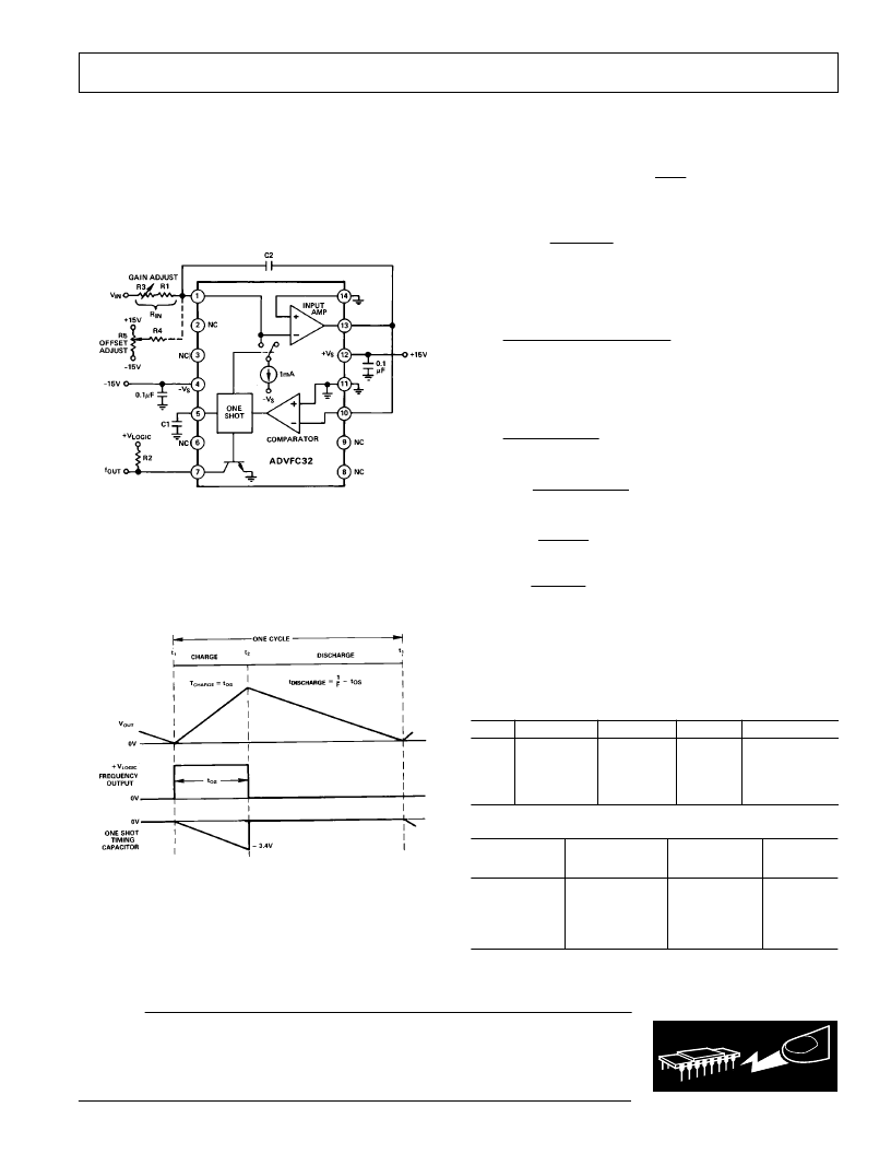
UNIPOLAR V/F, POSIT IVE INPUT VOLT AGE
When operated as a V/F converter, the transformation from
voltage to frequency is based on a comparison of input signal
magnitude to the 1 mA internal current source.
A more complete understanding of the ADVFC32 requires a
close examination of the internal circuitry of this part. Consider
the operation of the ADVFC32 when connected as shown in
Figure 1. At the start of a cycle, a current proportional to the
Figure 1. Connection Diagram for V/F Conversion,
Positive Input Voltage
input voltage flows through R3 and R1 to charge integration
capacitor C2. As charge builds up on C2, the output voltage of
the input amplifier decreases. When the amplifier output volt-
age (Pin 13) crosses ground (see Figure 2 at time t
1
), the
comparator triggers a one shot whose time period is determined
Figure 2. Voltage-to-Frequency Conversion Waveforms
by capacitor C1. Specifically, the one shot time period (in nano-
seconds) is:
t
OS
(
C
l
+ 44
pF
)
×
6.7
k
During this period, a current of (1 mA – I
IN
) flows out of the in-
tegration capacitor. T he total amount of charge depleted during
one cycle is, therefore (1 mA – I
IN
)
×
t
OS
. T his charge is replaced
during the remainder of the cycle to return the integrator to its
original voltage. Since the charge taken out of C2 is equal to the
charge that is put on C2 every cycle,
(
1
mA – I
IN
)
×
t
OS
= I
IN
×
1
F
OUT
±
t
OS
or, rearranging terms,
F
OUT
=
I
IN
1
mA
×
t
OS
T he complete transfer equation can now be derived by substi-
tuting I
IN
= V
IN
/R
IN
and the equation relating C1 and t
OS
. T he
final equation describing ADVFC32 operation is:
V
IIN
/
R
IN
1
mA
×
C
1
+
44
pF
(
Components should be selected to optimize performance over
the desired input voltage and output frequency range using the
equations listed below:
3.7
×
10
7
pF
/
sec
F
OUT FS
)
×
6.7
k
±44
pF
C
2
=
10
±4
Farads
/
sec
F
OUT FS
1000
pF minimum
(
)
R
IN
=
+
V
LOGIC
8
mA
V
IN FS
0.25
mA
R
2
≥
Both R
IN
and C
1
should have very low temperature coefficients
as changes in their values will result in a proportionate change in
the V/F transfer function. Other component values and tem-
perature coefficients are not critical.
WARNING!
ESD SENSITIVE DEVICE
C AUT ION
ESD (electrostatic discharge) sensitive device. Electrostatic charges as high as 4000 V readily
accumulate on the human body and test equipment and can discharge without detection.
Although the ADVFC32 features proprietary ESD protection circuitry, permanent damage may
occur on devices subjected to high energy electrostatic discharges. T herefore, proper ESD
precautions are recommended to avoid performance degradation or loss of functionality.
ORDE RING GUIDE
Part
Number
1
Gain T empco
ppm/
8
C
T emp Range
8
C
Package
Option
ADVFC32K N
±
75 typ
0 to +70
14-Pin
Plastic DIP
T O-100
T O-100
ADVFC32BH
ADVFC32SH
±
100 max
±
150 max
–25 to +85
–55 to +125
NOT E
1
For details on grade and package offerings screened in accordance with
MIL-ST D-883, refer to the Analog Devices Military Products Databook or current
ADVFC32/883B data sheet.
T able I. Suggested Values for C
1
, R
IN
and C
2
V
IN FS
1 V
10 V
1 V
10 V
F
OUT FS
10 kHz
10 kHz
100 kHz
100 kHz
C
1
3650 pF
3650 pF
330 pF
330 pF
R
IN
4.0 k
40 k
4.0 k
40 k
C
2
0.01
μ
F
0.01
μ
F
1000 pF
1000 pF
相關PDF資料 |
PDF描述 |
|---|---|
| ADVFC32SH | Voltage-to-Frequency and Frequency-to-Voltage Converter |
| ADXL105EM-1 | ADXL105/ADXL150/ADXL250/ADXL190 Evaluation Modules |
| ADXL105EM-3 | ADXL105/ADXL150/ADXL250/ADXL190 Evaluation Modules |
| ADXL150EM-1 | ADXL105/ADXL150/ADXL250/ADXL190 Evaluation Modules |
| ADXL150EM-3 | ADXL105/ADXL150/ADXL250/ADXL190 Evaluation Modules |
相關代理商/技術參數 |
參數描述 |
|---|---|
| ADVFC32KN/+ | 功能描述:IC CONVERTER V/F-F/V 14DIP RoHS:否 類別:集成電路 (IC) >> PMIC - V/F 和 F/V 轉換器 系列:- 標準包裝:1 系列:- 類型:頻率至電壓 頻率 - 最大:10kHz 全量程:- 線性:±0.3% 安裝類型:表面貼裝 封裝/外殼:8-SOIC(0.154",3.90mm 寬) 供應商設備封裝:8-SOIC 包裝:Digi-Reel® 其它名稱:LM2917MX-8/NOPBDKR |
| ADVFC32KNKL1 | 制造商:Analog Devices 功能描述: |
| ADVFC32KNZ | 功能描述:IC CONV V/F F/V 0-70DEGC 14DIP RoHS:是 類別:集成電路 (IC) >> PMIC - V/F 和 F/V 轉換器 系列:- 標準包裝:1 系列:- 類型:頻率至電壓 頻率 - 最大:10kHz 全量程:- 線性:±0.3% 安裝類型:表面貼裝 封裝/外殼:8-SOIC(0.154",3.90mm 寬) 供應商設備封裝:8-SOIC 包裝:Digi-Reel® 其它名稱:LM2917MX-8/NOPBDKR |
| ADVFC32SH | 功能描述:IC CONV V/F F/V MONO TO100-10 RoHS:否 類別:集成電路 (IC) >> PMIC - V/F 和 F/V 轉換器 系列:- 標準包裝:1 系列:- 類型:頻率至電壓 頻率 - 最大:10kHz 全量程:- 線性:±0.3% 安裝類型:表面貼裝 封裝/外殼:8-SOIC(0.154",3.90mm 寬) 供應商設備封裝:8-SOIC 包裝:Digi-Reel® 其它名稱:LM2917MX-8/NOPBDKR |
| ADVFC32SH/883B | 功能描述:電壓頻率轉換及頻率電壓轉換 IC MONO V/F AND F/V CONV RoHS:否 制造商:Texas Instruments 全標度頻率:4000 KHz 線性誤差:+/- 1 % FSR 電源電壓-最大: 電源電壓-最小: 最大工作溫度:+ 85 C 最小工作溫度:- 25 C 安裝風格:Through Hole 封裝 / 箱體:PDIP-14 封裝:Tube |
發布緊急采購,3分鐘左右您將得到回復。