- 您現在的位置:買賣IC網 > PDF目錄374049 > ADXL103CE1 (Analog Devices, Inc.) Precision 【1.7 g Single/Dual Axis Accelerometer PDF資料下載
參數資料
| 型號: | ADXL103CE1 |
| 廠商: | Analog Devices, Inc. |
| 英文描述: | Precision 【1.7 g Single/Dual Axis Accelerometer |
| 中文描述: | 精密【一點七克單/雙軸加速度計 |
| 文件頁數: | 8/12頁 |
| 文件大小: | 438K |
| 代理商: | ADXL103CE1 |
ADXL103/ADXL203
THEORY OF OPERATION
Rev. 0 | Page 8 of 12
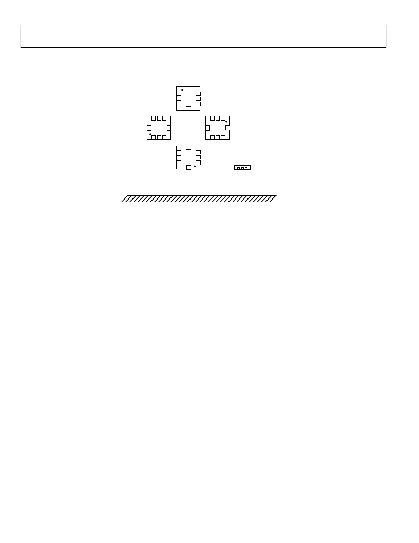
EARTH'S SURFACE
0
TOP VIEW
(Not to Scale)
PIN 8
X
OUT
= 2.5V
Y
OUT
= 1.5V
X
OUT
= 2.5V
Y
OUT
= 2.5V
PIN 8
X
OUT
= 2.5V
Y
OUT
= 3.5V
PIN 8
X
OUT
= 1.5V
Y
OUT
= 2.5V
PIN 8
X
OUT
= 3.5V
Y
OUT
= 2.5V
Figure 21. Output Response vs. Orientation
The ADXL103/ADXL203 are complete acceleration measure-
ment systems on a single monolithic IC. The ADXL103 is a
single axis accelerometer, while the ADXL203 is a dual axis
accelerometer. Both parts contain a polysilicon surface-
micromachined sensor and signal conditioning circuitry to
implement an open-loop acceleration measurement architec-
ture. The output signals are analog voltages proportional to
acceleration. The ADXL103/ADXL203 are capable of measuring
both positive and negative accelerations to at least ±1.7
g
. The
accelerometer can measure static acceleration forces such as
gravity, allowing it to be used as a tilt sensor.
The sensor is a surface-micromachined polysilicon structure
built on top of the silicon wafer. Polysilicon springs suspend the
structure over the surface of the wafer and provide a resistance
against acceleration forces. Deflection of the structure is mea-
sured using a differential capacitor that consists of independent
fixed plates and plates attached to the moving mass. The fixed
plates are driven by 180° out-of-phase square waves. Accelera-
tion will deflect the beam and unbalance the differential
capacitor, resulting in an output square wave whose amplitude
is proportional to acceleration. Phase sensitive demodulation
techniques are then used to rectify the signal and determine the
direction of the acceleration.
The output of the demodulator is amplified and brought off-
chip through a 32 k resistor. At this point, the user can set the
signal bandwidth of the device by adding a capacitor. This
filtering improves measurement resolution and helps prevent
aliasing.
PERFORMANCE
Rather than using additional temperature compensation
circuitry, innovative design techniques have been used to ensure
high performance is built in. As a result, there is essentially no
quantization error or non-monotonic behavior, and
temperature hysteresis is very low (typically less than 10 m
g
over the –40°C to +125°C temperature range).
Figure 9 shows the zero
g
output performance of eight parts (X
and Y axis) over a –40°C to +125°C temperature range.
Figure 12 demonstrates the typical sensitivity shift over
temperature for V
S
= 5 V. Sensitivity stability is optimized for
V
S
= 5 V, but is still very good over the specified range; it is
typically better than ±1% over temperature at V
S
= 3 V.
相關PDF資料 |
PDF描述 |
|---|---|
| ADXL204 | Precisionc +-1.7 g Single-/Dual-Axis i MEMS Accelerometer |
| ADXL204CE | Precisionc +-1.7 g Single-/Dual-Axis i MEMS Accelerometer |
| ADXL204CE-REEL | Precisionc +-1.7 g Single-/Dual-Axis i MEMS Accelerometer |
| ADXL204EB | Precisionc +-1.7 g Single-/Dual-Axis i MEMS Accelerometer |
| ADXL320EB | Small and Thin 5 g Accelerometer |
相關代理商/技術參數 |
參數描述 |
|---|---|
| ADXL103CE-REEL | 功能描述:IC ACCELEROMETER SNGL-AXIS 8CLCC RoHS:是 類別:傳感器,轉換器 >> 加速計 系列:iMEMS® 標準包裝:1 系列:SCA1000 軸:X,Y 加速范圍:±1.7g 靈敏度:1.2V/g 電源電壓:4.75 V ~ 5.25 V 輸出類型:數字 帶寬:50±30Hz 接口:SPI 安裝類型:表面貼裝 封裝/外殼:12-SMD 供應商設備封裝:12-SMD 其它名稱:551-1007-1 |
| ADXL103CE-REEL1 | 制造商:AD 制造商全稱:Analog Devices 功能描述:Precision 【1.7 g Single/Dual Axis Accelerometer |
| ADXL103WCEZB | 制造商:Analog Devices 功能描述: |
| ADXL103WCEZB-REEL | 制造商:Analog Devices 功能描述: 制造商:Analog Devices 功能描述:SENSOR |
| ADXL105 | 制造商:AD 制造商全稱:Analog Devices 功能描述:High Accuracy 61 g to 65 g Single Axis iMEMS Accelerometer with Analog Input |
發布緊急采購,3分鐘左右您將得到回復。