- 您現在的位置:買賣IC網 > PDF目錄3411 > ALD4704BPBL (Advanced Linear Devices Inc)IC OPAMP GP R-R CMOS QUAD 14PDIP PDF資料下載
參數資料
| 型號: | ALD4704BPBL |
| 廠商: | Advanced Linear Devices Inc |
| 文件頁數: | 1/9頁 |
| 文件大小: | 0K |
| 描述: | IC OPAMP GP R-R CMOS QUAD 14PDIP |
| 標準包裝: | 25 |
| 放大器類型: | 通用 |
| 電路數: | 4 |
| 輸出類型: | 推挽式,滿擺幅 |
| 轉換速率: | 5 V/µs |
| 增益帶寬積: | 2.1MHz |
| 電流 - 輸入偏壓: | 1pA |
| 電壓 - 輸入偏移: | 2000µV |
| 電流 - 電源: | 10mA |
| 電流 - 輸出 / 通道: | 15mA |
| 電壓 - 電源,單路/雙路(±): | 6.5 V ~ 12 V,±3.25 V ~ 6 V |
| 工作溫度: | 0°C ~ 70°C |
| 安裝類型: | 通孔 |
| 封裝/外殼: | 14-DIP(0.300",7.62mm) |
| 供應商設備封裝: | 14-PDIP |
| 包裝: | 管件 |
Rev 2.0 2010 Advanced Linear Devices, Inc. 415 Tasman Drive, Sunnyvale, CA 94089-1706 Tel: (408) 747-1155 Fax: (408) 747-1286
www.aldinc.com
QUAD RAIL-TO-RAIL CMOS OPERATIONAL AMPLIFIER
ALD4704A/ALD4704B
ALD4704
ADVANCED
LINEAR
DEVICES, INC.
Operating Temperature Range
0°C to +70°C0°C to +70°C
-55°C to 125°C
14-Pin
Small Outline
Plastic Dip
CERDIP
Package (SOIC)
Package
ALD4704ASBL
ALD4704APBL
ALD4704ADB
ALD4704BSBL
ALD4704BPBL
ALD4704BDB
ALD4704SBL
ALD4704PBL
ALD4704DB
* Contact factory for leaded (non-RoHS) or high temperature versions.
ORDERING INFORMATION (“L” suffix denotes lead-free (RoHS))
GENERAL DESCRIPTION
The ALD4704A/ALD4704B/ALD4704 is a dual monolithic operational
amplifier with MOSFET input that has rail-to-rail input and output voltage
ranges. The input voltage range and output voltage range are very close
to the positive and negative power supply voltages. Typically the input
voltage can be beyond positive power supply voltage V+ or the negative
power supply voltage V- by up to 300mV. The output voltage swings to
within 60mV of either positive or negative power supply voltages at rated
load.
With high impedance load,
the output voltage of the ALD4704A/
ALD4704B/ALD4704 approaches within 1mV of the power supply rails.
This device is designed as an alternative to the popular J-FET input
operational amplifier in applications where lower operating voltages,
such as 9V battery or ±3.25V to ±5V power supplies are being used. The
ALD4704A/ALD4704B/ALD4704 offers high slew rate of 5V/s. It is
designed and manufactured with Advanced Linear Devices' standard
enhanced ACMOS silicon gate CMOS process, and it offers low unit
cost and exceptional reliability.
The rail-to-rail input and output feature of the ALD4704A/ALD4704B/
ALD4704 expands signal voltage range for a given operating supply
voltage and allows numerous analog serial stages to be implemented
without losing operating voltage margin. The output stage is designed
to drive up to 10mA into 400pF capacitive and 1.5K resistive loads at
unity gain and up to 4000pF at a gain of 5. Short circuit protection to either
ground or the power supply rails is at approximately 15mA clamp
current. Due to complementary output stage design, the output can
source and sink 10mA into a load with symmetrical drive and is ideally
suited for applications where push-pull voltage drive is desired.
For each of the operational amplifier, the offset voltage is trimmed on-
chip to eliminate the need for external nulling in many applications. For
precision applications, the output is designed to settle to 0.1% in 2s. In
large signal buffer applications, the operational amplifier can function as
an ultrahigh input impedance voltage follower /buffer that allows input
and output voltage swings from positive to negative supply voltages.
This feature is intended to greatly simplify systems design and eliminate
higher voltage power supplies in many applications. Additionally, robust
design and rigorous screening make this device especially suitable for
operation in temperature-extreme environments and rugged conditions.
APPLICATIONS
Voltage amplifier
Voltage follower/buffer
Charge integrator
Photodiode amplifier
Data acquisition systems
High performance portable
instruments
Signal conditioning circuits
Low leakage amplifiers
Active filters
Sample/Hold amplifier
Picoammeter
Current to voltage converter
Coaxial cable driver
Capacitive sensor amplifier
Piezoelectric transducer amplifier
FEATURES
Rail-to-rail input and output voltage ranges
5.0V/s slew rate
Symmetrical push-pull output drive
Inputs can extend beyond supply rails by 300mV
Outputs settle to 2mV of supply rails
High capacitive load capability -- up to 4000pF
No frequency compensation required -- unity
gain stable
Extremely low input bias currents -- 1.0pA
typical (20pA max.)
Ideal for high source impedance applications
High voltage gain -- 100V/mV typical
Output short circuit protected
Unity gain bandwidth of 2.1MHz
Suitable for rugged, temperature-extreme
environments
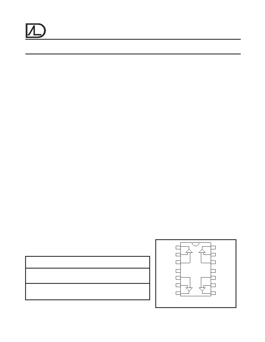
PIN CONFIGURATION
TOP VIEW
SBL, PBL, DB PACKAGES
OUT D
-IN D
+IN D
V-
+IN C
-IN C
OUT C
OUT A
-IN A
+IN A
V+
+IN B
-IN B
OUT B
1
2
3
4
5
6
7
8
9
10
11
12
13
14
相關PDF資料 |
PDF描述 |
|---|---|
| 961122-6700-AR-PT | CONN HEADER VERT 22POS GOLD SMD |
| TV06B130J-G | TVS 600W 13V UNIDIRECT 5% SMB |
| ALD4702BPBL | IC OPAMP GP R-R CMOS QUAD 14PDIP |
| TV06B120J-HF | TVS 600W 12V UNIDIRECT 5% SMB |
| ALD4704BSBL | IC OPAMP GP R-R CMOS QUAD 14SOIC |
相關代理商/技術參數 |
參數描述 |
|---|---|
| ALD4704BSB | 功能描述:運算放大器 - 運放 High Slew Rate RoHS:否 制造商:STMicroelectronics 通道數量:4 共模抑制比(最小值):63 dB 輸入補償電壓:1 mV 輸入偏流(最大值):10 pA 工作電源電壓:2.7 V to 5.5 V 安裝風格:SMD/SMT 封裝 / 箱體:QFN-16 轉換速度:0.89 V/us 關閉:No 輸出電流:55 mA 最大工作溫度:+ 125 C 封裝:Reel |
| ALD4704BSBL | 功能描述:運算放大器 - 運放 2.0mV High Slew Rate RoHS:否 制造商:STMicroelectronics 通道數量:4 共模抑制比(最小值):63 dB 輸入補償電壓:1 mV 輸入偏流(最大值):10 pA 工作電源電壓:2.7 V to 5.5 V 安裝風格:SMD/SMT 封裝 / 箱體:QFN-16 轉換速度:0.89 V/us 關閉:No 輸出電流:55 mA 最大工作溫度:+ 125 C 封裝:Reel |
| ALD4704DB | 制造商:未知廠家 制造商全稱:未知廠家 功能描述:Operational Amplifier |
| ALD4704PB | 功能描述:運算放大器 - 運放 High Slew Rate RoHS:否 制造商:STMicroelectronics 通道數量:4 共模抑制比(最小值):63 dB 輸入補償電壓:1 mV 輸入偏流(最大值):10 pA 工作電源電壓:2.7 V to 5.5 V 安裝風格:SMD/SMT 封裝 / 箱體:QFN-16 轉換速度:0.89 V/us 關閉:No 輸出電流:55 mA 最大工作溫度:+ 125 C 封裝:Reel |
| ALD4704PBL | 功能描述:運算放大器 - 運放 5.0mV High Slew Rate RoHS:否 制造商:STMicroelectronics 通道數量:4 共模抑制比(最小值):63 dB 輸入補償電壓:1 mV 輸入偏流(最大值):10 pA 工作電源電壓:2.7 V to 5.5 V 安裝風格:SMD/SMT 封裝 / 箱體:QFN-16 轉換速度:0.89 V/us 關閉:No 輸出電流:55 mA 最大工作溫度:+ 125 C 封裝:Reel |
發布緊急采購,3分鐘左右您將得到回復。