- 您現在的位置:買賣IC網 > PDF目錄379669 > AN231E04-E2-QFNTY (Electronic Theatre Controls, Inc.) Dynamically Reconfigurable dpASP PDF資料下載
參數資料
| 型號: | AN231E04-E2-QFNTY |
| 廠商: | Electronic Theatre Controls, Inc. |
| 英文描述: | Dynamically Reconfigurable dpASP |
| 中文描述: | 動態可重構dpASP |
| 文件頁數: | 4/24頁 |
| 文件大小: | 445K |
| 代理商: | AN231E04-E2-QFNTY |
AN231E04 Datasheet – Dynamically Reconfigurable dpASP
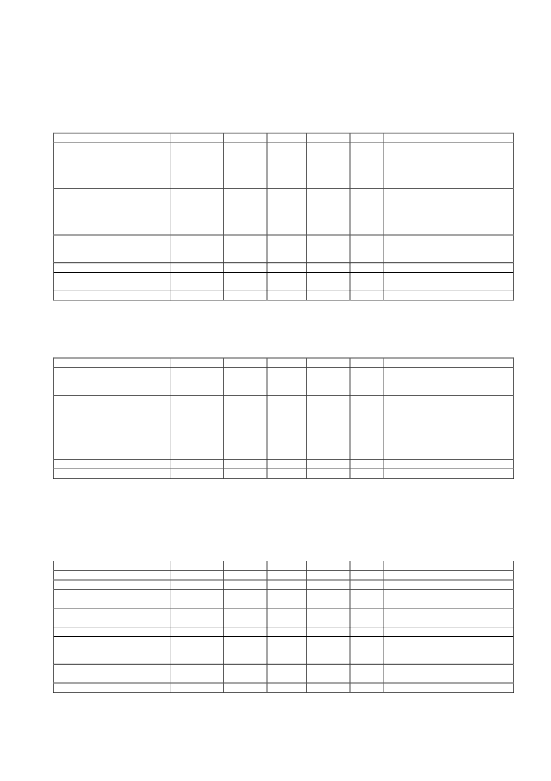
ELECTRICAL CHARACTERISTICS
DS231000-U001d
- 4 -
1
1.1
Absolute Maximum Ratings
Parameter
DC Power Supplies
a
Symbol
AVDD
BVDD
DVDD
Min
Typ
Max
Unit
Comment
-0.5
-
3.6 V
V
AVSS, BVSS and DVSS all held
to 0.0 V
xVDD to yVDD Offset
-0.5
0.5
V
Ideally all supplies should be at
the same voltage
(Theoretical values based on
Tj=125deg.C)
Still air, No heatsink, 44 pads and
exposed die pad soldered to PCB
θ
ja = 22.5°C/W. VDD = 3.3V
Maximum power dissipation all
resources used, (see section
1.5.13 for more detail).
Package Power Dissipation,
Pmax 25°C
Pmax 85°C
-
-
4.5
1.8
W
AN231E04 max power
dissipation
dpASPmax
-
-
0.25
W
Input Voltage
Ambient Operating
Temperature
Storage Temperature
Vinmax
VSS-0.5
-
VDD+0.5
V
Top
-40
-
85
°C
°C
Tstg
-40
125
a
Absolute Maximum DC Power Supply Rating - The failure mode is non-catastrophic for VDD of up to 5 volts, but will cause
reduced operating life time. The additional stress caused by higher local electric fields within the CMOS circuitry may induce
metal migration, oxide leakage and other time/quality related issues.
1.2
Recommended Operating Conditions
Parameter
Symbol
AVDD
BVDD
DVDD
Min
Typ
Max
Unit
Comment
DC Power Supplies
3.0
3.3
3.6
V
AVSS, BVSS and DVSS all held
to 0 V
Analog Input Voltage.
Vina
VMR
-1.375
-
VMR
+1.375
V
Conditional on the circuit which is
being driven. This limit is defined
as maximum signal amplitude
through input Sample and hold
cell which results in >-80dB
THD+N using a 1KHz test signal.
VMR is 1.5 volts above AVSS
Assume a package
θ
ja=22.5°C/W
Digital Input Voltage
Junction Temp
b
Vind
Tj
0
-
-
DVDD
125
V
°C
-40
b
To calculate the junction temperature (Tj) you must first empirically determine the current draw (total Idd) for the design. The
programmable nature of this device means this can vary by orders of magnitude between different circuit designs. Once the current
consumption is established then the following formula can be used; Tj = Ta + Idd x VDD x 22.5 °C/W, where Ta is the ambient
temperature. Worst case
θ
ja = 22.5 °C/W assumes no air flow and no additional heatsink, 44 pads and the exposed die pad soldered
to PCB.
1.3
General Digital I/O Characteristics (VDD = 3.3v +/- 10%, -40 to 85 deg.C)
Parameter
Symbol
Input Voltage Low
Vih
Input Voltage High
Vil
Output Voltage Low
Vol
Output Voltage High
Voh
Min
0
70
0
80
Typ
-
-
-
-
Max
30
100
20
100
Unit
-
-
-
-
Comment
% of DVDD
% of DVDD
% of DVDD
% of DVDD
Some pins have active pull
up/down, please see below.
Each pins has a specific load
driving capability, detailed in
sections 1.4 and 1.5
Divide down to <4 MHz prior to
use as a CAB clock
All clocks
Input Leakage Current
Iil
-
-
+/-1
μA
pF
Max. Capacitive Load
Cmax
-
-
10
Min. Resistive Load
Rmin
50
-
-
Kohm
ACLK Frequency
Fmax
-
16
40
MHz
Clock Duty Cycle
CLKduty
45
-
55
%
相關PDF資料 |
PDF描述 |
|---|---|
| AN231K04-DVLP3 | Dynamically Reconfigurable dpASP |
| AN321 | AND / NOR circuit providing the logical function |
| AN3791 | VTR X-VALUE SHIFT CIRCUIT |
| AN53 | The CS5322 Digital Filter |
| AN7203 | FM FRONT-END IC FOR RADIO, RADIO CASSETTE RECORDER |
相關代理商/技術參數 |
參數描述 |
|---|---|
| AN231K04-DVLP3 | 制造商:未知廠家 制造商全稱:未知廠家 功能描述:Dynamically Reconfigurable dpASP |
| AN232 | 制造商:MICROCHIP 制造商全稱:Microchip Technology 功能描述:Low Frequency Magnetic Transmitter Design |
| AN2320S | 制造商:未知廠家 制造商全稱:未知廠家 功能描述:Video Camera Circuit |
| AN23-23A | 制造商:AN# - MILITARY 功能描述: |
| AN23-25A | 制造商:AN# - MILITARY 功能描述: |
發布緊急采購,3分鐘左右您將得到回復。