- 您現在的位置:買賣IC網 > PDF目錄379696 > ATT3020-50T84I (Electronic Theatre Controls, Inc.) Field-Programmable Gate Arrays PDF資料下載
參數資料
| 型號: | ATT3020-50T84I |
| 廠商: | Electronic Theatre Controls, Inc. |
| 元件分類: | FPGA |
| 英文描述: | Field-Programmable Gate Arrays |
| 中文描述: | 現場可編程門陣列 |
| 文件頁數: | 29/80頁 |
| 文件大小: | 528K |
| 代理商: | ATT3020-50T84I |
第1頁第2頁第3頁第4頁第5頁第6頁第7頁第8頁第9頁第10頁第11頁第12頁第13頁第14頁第15頁第16頁第17頁第18頁第19頁第20頁第21頁第22頁第23頁第24頁第25頁第26頁第27頁第28頁當前第29頁第30頁第31頁第32頁第33頁第34頁第35頁第36頁第37頁第38頁第39頁第40頁第41頁第42頁第43頁第44頁第45頁第46頁第47頁第48頁第49頁第50頁第51頁第52頁第53頁第54頁第55頁第56頁第57頁第58頁第59頁第60頁第61頁第62頁第63頁第64頁第65頁第66頁第67頁第68頁第69頁第70頁第71頁第72頁第73頁第74頁第75頁第76頁第77頁第78頁第79頁第80頁
Data Sheet
February 1997
ATT3000 Series Field-Programmable Gate Arrays
Lucent Technologies Inc.
29
Performance
Device Performance
The high performance of the FPGA is due in part to the
manufacturing process, which is similar to that used for
high-speed CMOS static memories. Performance can
be measured in terms of minimum propagation times
for logic elements. The parameter which traditionally
describes the overall performance of a gate array is the
toggle frequency of a flip-flop. The configuration for
determining the toggle performance of the FPGA is
shown in Figure 26. The flip-flop output Q is fed back
through the combinatorial logic as Q to form the toggle
flip-flop.
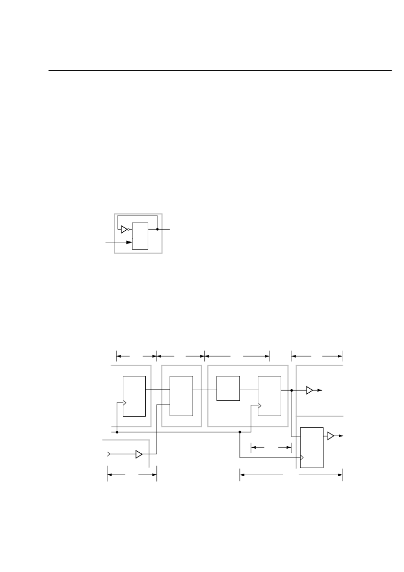
Figure 26. Toggle Flip-Flop
FPGA performance is determined by the timing of
critical paths, including both the fixed timing for the
logic and storage elements in that path, and the timing
associated with the routing of the network. Examples
of internal worst-case timing are included in the
performance data to allow the user to make the best
use of the capabilities of the device. The
ORCA
Foundry Development System timing calculator or
ORCA
Foundry-generated simulation models should
be used to calculate worst-case paths by using actual
impedance and loading information.
Figure 27 shows a variety of elements which are
involved in determining system performance. Table 20
gives the parameter values for the different speed
grades. Actual measurement of internal timing is not
practical, and often only the sum of component
timing is relevant as in the case of input to output. The
relationship between input and output timing is arbi-
trary, and only the total determines performance.
Timing components of internal functions may be deter-
mined by the measurement of differences at the pins of
the package. A synchronous logic function which
involves a clock to block-output and a block-input to
clock setup is capable of higher-speed operation than a
logic configuration of two synchronous blocks with an
extra combinatorial block level between them. System
clock rates to 60% of the toggle frequency are practical
for logic in which an extra combinatorial level is located
between synchronized blocks. This allows implementa-
tion of functions of up to 25 variables. The use of the
wired-AND is also available for wide, high-speed
functions.
CLOCK
D Q
5-3117(F)
Figure 27. Examples of Primary Block Speed Factors
CLOCK
LOGIC
LOGIC
CLB
CLB
CLB
(K)
(K)
IOB
PAD
T
CKO
T
ILO
T
ICK
T
OP
CLOCK TO
OUTPUT
COMBINATORIAL
SETUP
IOB
T
PID
T
OKOP
T
CKO
PAD
5-3118(F)
相關PDF資料 |
PDF描述 |
|---|---|
| ATT3020-70H132I | Field-Programmable Gate Arrays |
| ATT3020-70H44I | Field-Programmable Gate Arrays |
| ATT3020-70H68I | Field-Programmable Gate Arrays |
| ATT3020-70H84I | Field-Programmable Gate Arrays |
| ATT3020-70J132I | Field-Programmable Gate Arrays |
相關代理商/技術參數 |
參數描述 |
|---|---|
| ATT3020-5J100I | 制造商:未知廠家 制造商全稱:未知廠家 功能描述:Field Programmable Gate Array (FPGA) |
| ATT3020-5M68I | 制造商:未知廠家 制造商全稱:未知廠家 功能描述:Field Programmable Gate Array (FPGA) |
| ATT3020-5M84I | 制造商:未知廠家 制造商全稱:未知廠家 功能描述:Field Programmable Gate Array (FPGA) |
| ATT3020-70H132I | 制造商:未知廠家 制造商全稱:未知廠家 功能描述:Field-Programmable Gate Arrays |
| ATT3020-70H44I | 制造商:未知廠家 制造商全稱:未知廠家 功能描述:Field-Programmable Gate Arrays |
發布緊急采購,3分鐘左右您將得到回復。