- 您現(xiàn)在的位置:買賣IC網(wǎng) > PDF目錄379700 > ATT3030-50J132I (Electronic Theatre Controls, Inc.) Field-Programmable Gate Arrays PDF資料下載
參數(shù)資料
| 型號: | ATT3030-50J132I |
| 廠商: | Electronic Theatre Controls, Inc. |
| 元件分類: | FPGA |
| 英文描述: | Field-Programmable Gate Arrays |
| 中文描述: | 現(xiàn)場可編程門陣列 |
| 文件頁數(shù): | 59/80頁 |
| 文件大小: | 528K |
| 代理商: | ATT3030-50J132I |
第1頁第2頁第3頁第4頁第5頁第6頁第7頁第8頁第9頁第10頁第11頁第12頁第13頁第14頁第15頁第16頁第17頁第18頁第19頁第20頁第21頁第22頁第23頁第24頁第25頁第26頁第27頁第28頁第29頁第30頁第31頁第32頁第33頁第34頁第35頁第36頁第37頁第38頁第39頁第40頁第41頁第42頁第43頁第44頁第45頁第46頁第47頁第48頁第49頁第50頁第51頁第52頁第53頁第54頁第55頁第56頁第57頁第58頁當(dāng)前第59頁第60頁第61頁第62頁第63頁第64頁第65頁第66頁第67頁第68頁第69頁第70頁第71頁第72頁第73頁第74頁第75頁第76頁第77頁第78頁第79頁第80頁
Data Sheet
February 1997
ATT3000 Series Field-Programmable Gate Arrays
Lucent Technologies Inc.
59
Electrical Characteristics
(continued)
* These parameters are for clock pulses within an FPGA device. For externally applied clock, increase values by 20%.
Notes:
Timing is measured at pin threshold with 50 pF external capacitive loads (including test fixture).
Typical fast mode output rise/fall times are 2 ns and will increase approximately 2%/pF of additional load.
Typical slew-rate limited output rise/fall times are approximately 4 times longer.
A maximum total external capacitive load for simultaneous fast mode switching in the same direction is 200 pF per power/ground pin pair. For
slew-rate limited outputs, this total is 4 times larger. Exceeding this maximum capacitive load can result in ground bounce of >1.5 V amplitude
and <5 ns duration, which may cause problems when the FPGA drives clocks and other asynchronous signals.
Voltage levels of unused (bonded and unbonded) pads must be valid logic levels. Each can be configured with the internal pull-up resistor or
alternatively configured as a driven output or driven from an external source.
Input pad setup time is specified with respect to the internal clock (ik).
To calculate system setup time, subtract clock delay (pad to ik) from the input pad setup time value. Input pad hold time with respect to the
internal clock (ik) is negative. This means that pad levels changed immediately before the internal clock edge (ik) will not be recognized.
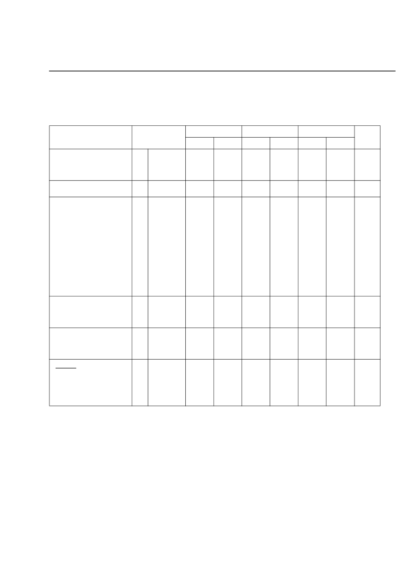
Table 23. IOB Switching Characteristics (-3, -4, and -5)
Commercial: V
CC
= 5.0 V ± 5%; 0 °C
≤
T
A
≤
70 °C; Industrial: V
CC
= 5.0 ± 10%, –40 °C
≤
T
A
≤
+85 °C.
Description
Symbol
-5
-4
-3
Unit
Min
Max
Min
Max
Min
Max
Input Delays
Pad to Direct In
Pad to Registered In
Clock to Registered In
Setup Time (Input):
Clock Setup Time
Output Delays
Clock to Pad
Fast
Slew-rate Limited
Output to Pad
Fast
Slew-rate Limited
3-state to Pad Hi-Z
Fast
Slew-rate Limited
3-state to Pad Valid
Fast
Slew-rate Limited
Setup and Hold Times
(output)
Clock Setup Time
Clock Hold Time
Clock
High Time*
Low Time*
Max. Flip-Flop Toggle*
Master Reset Delays
RESET to:
Registered In
Output Pad (fast)
Output Pad (slew-
rate limited)
3
—
4
T
PID
T
PTG
T
IKRI
—
—
—
2.8
16.0
2.8
—
—
—
2.5
15.0
2.5
—
—
—
2.2
13.0
2.2
ns
ns
ns
1
T
PICK
15.0
—
14.0
—
12.0
—
ns
7
7
10
10
9
9
8
8
T
OKPO
T
OKPO
T
OPF
T
OPS
T
TSHZ
T
TSHZ
T
TSON
T
TSON
—
—
—
—
—
—
—
—
5.5
14.0
4.1
13.0
6.9
21.0
12.0
20.0
—
—
—
—
—
—
—
—
5.0
12.0
3.7
11.0
6.2
19.0
10.0
17.0
—
—
—
—
—
—
—
—
4.4
10.0
3.3
9.0
5.5
17.0
9.0
15.0
ns
ns
ns
ns
ns
ns
ns
ns
5
6
T
OCK
T
OKO
6.2
0
—
—
5.6
0
—
—
5.0
0
—
—
ns
ns
11
12
—
T
CH
T
CL
F
CLK
2.4
2.4
190
—
—
—
2.0
2.0
230
—
—
—
1.6
1.6
270
—
—
—
ns
ns
MHz
13
15
15
T
RRI
T
RPO
T
RPO
—
—
—
18
24
32
—
—
—
15
20
27
—
—
—
13
17
23
ns
ns
ns
相關(guān)PDF資料 |
PDF描述 |
|---|---|
| ATT3030-50J44I | Field-Programmable Gate Arrays |
| ATT3030-50J68I | Field-Programmable Gate Arrays |
| ATT3030-50J84I | Field-Programmable Gate Arrays |
| ATT3030-50M132I | Field-Programmable Gate Arrays |
| ATT3030-50M44I | Field-Programmable Gate Arrays |
相關(guān)代理商/技術(shù)參數(shù) |
參數(shù)描述 |
|---|---|
| ATT3030-50J44I | 制造商:未知廠家 制造商全稱:未知廠家 功能描述:Field-Programmable Gate Arrays |
| ATT3030-50J68I | 制造商:未知廠家 制造商全稱:未知廠家 功能描述:Field-Programmable Gate Arrays |
| ATT3030-50J84I | 制造商:未知廠家 制造商全稱:未知廠家 功能描述:Field-Programmable Gate Arrays |
| ATT3030-50M132I | 制造商:未知廠家 制造商全稱:未知廠家 功能描述:Field-Programmable Gate Arrays |
| ATT3030-50M44I | 制造商:未知廠家 制造商全稱:未知廠家 功能描述:Field-Programmable Gate Arrays |
發(fā)布緊急采購,3分鐘左右您將得到回復(fù)。