- 您現在的位置:買賣IC網 > PDF目錄379701 > ATT3042-190M68I (Electronic Theatre Controls, Inc.) Field-Programmable Gate Arrays PDF資料下載
參數資料
| 型號: | ATT3042-190M68I |
| 廠商: | Electronic Theatre Controls, Inc. |
| 元件分類: | FPGA |
| 英文描述: | Field-Programmable Gate Arrays |
| 中文描述: | 現場可編程門陣列 |
| 文件頁數: | 14/80頁 |
| 文件大小: | 528K |
| 代理商: | ATT3042-190M68I |
第1頁第2頁第3頁第4頁第5頁第6頁第7頁第8頁第9頁第10頁第11頁第12頁第13頁當前第14頁第15頁第16頁第17頁第18頁第19頁第20頁第21頁第22頁第23頁第24頁第25頁第26頁第27頁第28頁第29頁第30頁第31頁第32頁第33頁第34頁第35頁第36頁第37頁第38頁第39頁第40頁第41頁第42頁第43頁第44頁第45頁第46頁第47頁第48頁第49頁第50頁第51頁第52頁第53頁第54頁第55頁第56頁第57頁第58頁第59頁第60頁第61頁第62頁第63頁第64頁第65頁第66頁第67頁第68頁第69頁第70頁第71頁第72頁第73頁第74頁第75頁第76頁第77頁第78頁第79頁第80頁
Data Sheet
February 1997
ATT3000 Series Field-Programmable Gate Arrays
14
Lucent Technologies Inc.
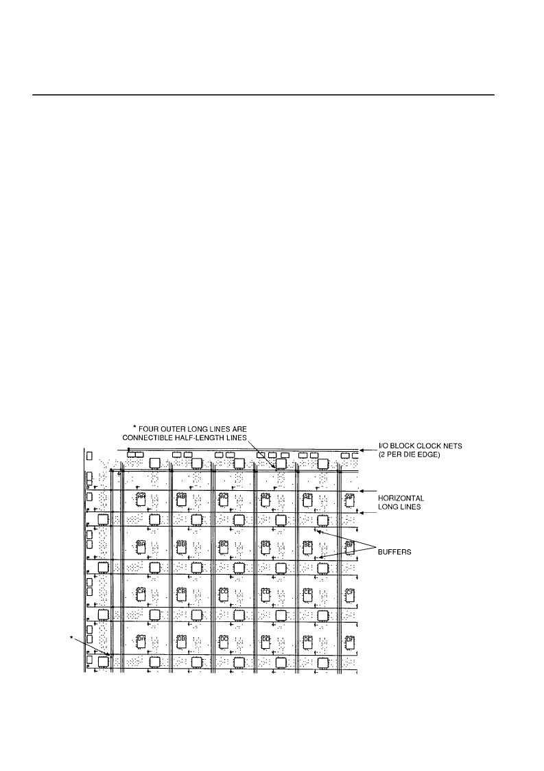
Programmable Interconnect
(continued)
A buffer in the upper left corner of the FPGA chip drives
a global net which is available to all .k inputs of logic
blocks. Using the global buffer for a clock signal pro-
vides a skew-free, high fan-out, synchronized clock for
use at any or all of the I/O and logic blocks. Configura-
tion bits for the .k input to each logic block can select
this global line, or another routing resource, as the
clock source for its flip-flops. This net may also be pro-
grammed to drive the die edge clock lines for IOB use.
An enhanced speed, CMOS threshold, offers direct
access to this buffer and is available at the
second pad from the top of the left die edge.
A buffer in the lower right corner of the array drives a
horizontal long line that can drive programmed connec-
tions to a vertical long line in each interconnection
column. This alternate buffer also has low skew and
high fan-out. The network formed by this alternate buf-
fer’s long lines can be selected to drive the .k inputs of
the logic blocks. CMOS threshold, high-speed access
to this buffer is available from the third pad from the
bottom of the right die edge.
Internal Buses
A pair of 3-state buffers is located adjacent to each
CLB. These buffers allow logic to drive the horizontal
long lines. Logical operation of the 3-state buffer
controls allows them to implement wide multiplexing
functions. Any 3-state buffer input can be selected as
drive for the horizontal long line bus by applying a low
logic level on its 3-state control line (see Figure 15A).
The user is required to avoid contention that can result
from multiple drivers with opposing logic levels. Control
of the 3-state input by the same signal that drives the
buffer input creates an open-drain wired-AND function.
A logical high on both buffer inputs creates a high
impedance which represents no contention. A logical
low enables the buffer to drive the long line low (see
Figure 15B). Pull-up resistors are available at each end
of the long line to provide a high output when all con-
nected buffers are nonconducting. This forms fast, wide
gating functions. When data drives the inputs and sep-
arate signals drive the 3-state control lines, these buff-
ers form multiplexers (3-state buses). In this case, care
must be used to prevent contention through multiple
active buffers of conflicting levels on a common line.
Figure 16 shows 3-state buffers, long lines, and pull-up
resistors.
Figure 14. Programmable Interconnection of Long Lines
3-STATE
相關PDF資料 |
PDF描述 |
|---|---|
| ATT3042-190M84I | Field-Programmable Gate Arrays |
| ATT3042-190S132I | Field-Programmable Gate Arrays |
| ATT3042-190S44I | Field-Programmable Gate Arrays |
| ATT3042-190S68I | Field-Programmable Gate Arrays |
| ATT3042-190S84I | Field-Programmable Gate Arrays |
相關代理商/技術參數 |
參數描述 |
|---|---|
| ATT3042-190M84I | 制造商:未知廠家 制造商全稱:未知廠家 功能描述:Field-Programmable Gate Arrays |
| ATT3042-190S132I | 制造商:未知廠家 制造商全稱:未知廠家 功能描述:Field-Programmable Gate Arrays |
| ATT3042-190S44I | 制造商:未知廠家 制造商全稱:未知廠家 功能描述:Field-Programmable Gate Arrays |
| ATT3042-190S68I | 制造商:未知廠家 制造商全稱:未知廠家 功能描述:Field-Programmable Gate Arrays |
| ATT3042-190S84I | 制造商:未知廠家 制造商全稱:未知廠家 功能描述:Field-Programmable Gate Arrays |
發布緊急采購,3分鐘左右您將得到回復。