- 您現(xiàn)在的位置:買賣IC網(wǎng) > Datasheet目錄39 > BD3504FVM-TR (Rohm Semiconductor)IC REG CTRLR SGL POS ADJ 8MSOP Datasheet資料下載
參數(shù)資料
| 型號: | BD3504FVM-TR |
| 廠商: | Rohm Semiconductor |
| 文件頁數(shù): | 13/19頁 |
| 文件大小: | 605K |
| 描述: | IC REG CTRLR SGL POS ADJ 8MSOP |
| 標準包裝: | 2,000 |
| 類型: | 正,可調(diào)式 |
| 輸出數(shù): | 1 |
| 輸出電壓: | 0.65 V ~ 2.5 V |
| 輸入電壓: | 4.5 V ~ 5.5 V |
| 工作溫度: | -10°C ~ 100°C |
| 封裝/外殼: | 8-VSSOP,8-MSOP(0.118",3.00mm 寬) |
| 供應(yīng)商設(shè)備封裝: | 8-MSOP |
| 包裝: | 帶卷 (TR) |
BD3504FVM,BD3500FVM,BD3501FVM,BD3502FVM
Technical Note
13/16
www.rohm.com
2010.05 - Rev.A
?2010 ROHM Co., Ltd. All rights reserved.
?SPAN class="pst BD3504FVM-TR_2649171_6">Notes for use
1. Absolute maximum ratings
For the present product, thoroughgoing quality control is carried out, but in the event that applied voltage, working
temperature range, and other absolute maximum rating are exceeded, the present product may be destroyed. Because
it is unable to identify the short mode, open mode, etc., if any special mode is assumed, which exceeds the absolute
maximum rating, physical safety measures are requested to be taken, such as fuses, etc.
2. GND potential
Bring the GND terminal potential to the minimum potential in any operating condition.
3. Thermal design
Consider allowable loss (Pd) under actual working condition and carry out thermal design with sufficient margin provided.
4. Terminal-to-terminal short-circuit and erroneous mounting
When the present IC is mounted to a printed circuit board, take utmost care to direction of IC and displacement. In the
event that the IC is mounted erroneously, IC may be destroyed. In the event of short-circuit caused by foreign matter that
enters in a clearance between outputs or output and power-GND, the IC may be destroyed.
5. Operation in strong electromagnetic field
The use of the present IC in the strong electromagnetic field may result in maloperation, to which care must be taken.
6. Built-in thermal shutdown protection circuit
The present IC incorporates a thermal shutdown protection circuit (TSD circuit). The working temperature is 175癈
(standard value) and has a -15 (standard value) hysteresis width. When the IC chip temperature rises and the TSD
circuit operates, the output terminal is brought to the OFF state. The built-in thermal shutdown protection circuit (TSD
circuit) is first and foremost intended for interrupt IC from thermal runaway, and is not intended to protect and warrant the
IC. Consequently, never attempt to continuously use the IC after this circuit is activated or to use the circuit with the
activation of the circuit premised.
7. Capacitor across output and GND
In the event a large capacitor is connected across output and GND, when Vcc and VIN are short-circuited with 0V or GND
for some kind of reasons, current charged in the capacitor flows into the output and may destroy the IC. Use a capacitor
smaller than 1000 礔 between output and GND.
8. Inspection by set substrate
In the event a capacitor is connected to a pin with low impedance at the time of inspection with a set substrate, there is a
fear of applying stress to the IC. Therefore, be sure to discharge electricity for every process. As electrostatic
measures, provide grounding in the assembly process, and take utmost care in transportation and storage. Furthermore,
when the set substrate is connected to a jig in the inspection process, be sure to turn OFF power supply to connect the jig
and be sure to turn OFF power supply to remove the jig.
9. IC terminal input
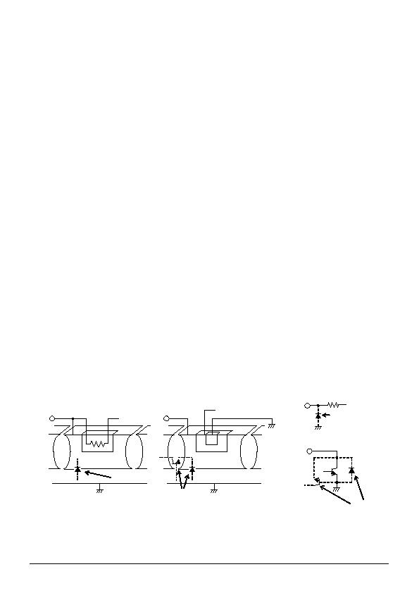
The present IC is a monolithic IC and has a P substrate and P+ isolation between elements.
With this P layer and N layer of each element, PN junction is formed, and when the potential relation is
桮ND>terminal A>terminal B, PN junction works as a diode, and
梩erminal B>GND terminal A, PN junction operates as a parasitic transistor.
The parasitic element is inevitably formed because of the IC construction. The operation of the parasitic element gives
rise to mutual interference between circuits and results in malfunction, and eventually, breakdown. Consequently, take
utmost care not to use the IC to operate the parasitic element such as applying voltage lower than GND (P substrate) to
the input terminal.
(PIN A)
P+
P+
N
N
N
P
P substrate
GND
GND
N
P
N
C
B
E
GND
P+
P+
N
N
Resistor
NPN Transistor Structure (NPN)
(PIN B)
Parasitic diode
GND
(PIN A)
C
E
B
GND
Nearby other device
(PIN B)
Parasitic diode
Parasitic diode
Parasitic diode
P substrate
相關(guān)PDF資料 |
PDF描述 |
|---|---|
| BD3521FVM-TR | IC REG CTRLR SGL 1.5V MSOP8 |
| BD9153MUV-E2 | IC REG TRPL BCK/LINEAR 24VQFN |
| CAT2300VP2-GT3 | IC SENSE FET CONTROLLER 8TDFN |
| CAT34TS02VP2GT4A | IC TEMP SENSOR 2K MEMORY 8TDFN |
| CAT6095VP2-GT4 | IC TEMP SENSOR STAND ALONE 8TDFN |
相關(guān)代理商/技術(shù)參數(shù) |
參數(shù)描述 |
|---|---|
| BD3505 | 制造商:WTE 制造商全稱:Won-Top Electronics 功能描述:35A BOSCH TYPE PRESS-FIT DIODE |
| BD3506 | 制造商:WTE 制造商全稱:Won-Top Electronics 功能描述:35A BOSCH TYPE PRESS-FIT DIODE |
| BD3506EFV | 制造商:ROHM 制造商全稱:Rohm 功能描述:Nch FET Ultra LDO for PC Chipsets |
| BD3506F | 制造商:ROHM 制造商全稱:Rohm 功能描述:Nch FET Ultra LDO for PC Chipsets |
| BD3506F_08 | 制造商:ROHM 制造商全稱:Rohm 功能描述:Ultra Low Dropout Linear Regulators for PC Chipsets |
發(fā)布緊急采購,3分鐘左右您將得到回復(fù)。