- 您現(xiàn)在的位置:買賣IC網(wǎng) > PDF目錄379728 > CA3256 (Intersil Corporation) 25MHz, BiMOS Analog Video Switch and Amplifier PDF資料下載
參數(shù)資料
| 型號: | CA3256 |
| 廠商: | Intersil Corporation |
| 英文描述: | 25MHz, BiMOS Analog Video Switch and Amplifier |
| 中文描述: | 高達25MHz,BiMOS模擬視頻開關(guān)和放大器 |
| 文件頁數(shù): | 1/11頁 |
| 文件大小: | 389K |
| 代理商: | CA3256 |
8-1
Semiconductor
January 1999
CA3256
25MHz, BiMOS Analog
Video Switch and Amplifier
CAUTION: These devices are sensitive to electrostatic discharge. Users should follow proper IC Handling Procedures.
Copyright
Harris Corporation 1999
File Number
1769.5
Features
5 Multiplex Video Channels
- 1 Independent Channel
- 4 Channels with Enable
4 LED Channel Indicator Outputs
Wideband Video Amplifier . . . . . . . .25MHz Unity Gain
Adjustable Video Amplifier Gain
High Signal-Drive Capability
Applications
Video Multiplex Switch
75
Video Amplifier/Line Driver
Video Signal-Level Control
Monitor Switching Control
TV/CATV Audio/Video Switch
Video Signal Adder/Fader Control
Description
The CA3256 BiMOS analog video switch has five channels
of CMOS multiplex switching for general-purpose video-
signal control. One of four CMOS channels may be selected
in parallel with channel 5. The CMOS switches are inputs to
the video amplifier but may be used in bilateral switching
between channels 1 to 4 and channel 5. The analog
switches of channels 1 to 4 are digitally controlled with logic
level conversion and binary decoding to select 1 of 4
channels. The enable function controls channels 1 to 4 but
does not affect channel 5. LED output drivers are selected
with the channel 1-to-4 switch selection to indicate the ON-
channel. Channel 5 may be used as a monitor output for
data or signal information on channels 1 to 4. The
transmission gate switches shown in the block diagram of
the CA3256 are configured in a “T” design to minimize
feedthrough. When the switch is off, the shunt or center of
the “T” is grounded.
The amplifier has high input impedance to minimize the R
ON
transmission gate insertion loss. The amplifier output imped-
ance is typically 5
in a complementary symmetry output.
The amplifier can directly drive a nominal 75
coaxial cable
to provide line-to-line video switching. The gain of the ampli-
fier is programmable by different feedback resistor values
between pins 8 and 9. Compensation may also be used
between these pins for an optimally flat frequency response.
An internal regulated 5V bias reference with temperature
compensation permits stable direct-coupled output drive and
minimizes DC offset during signal switching.
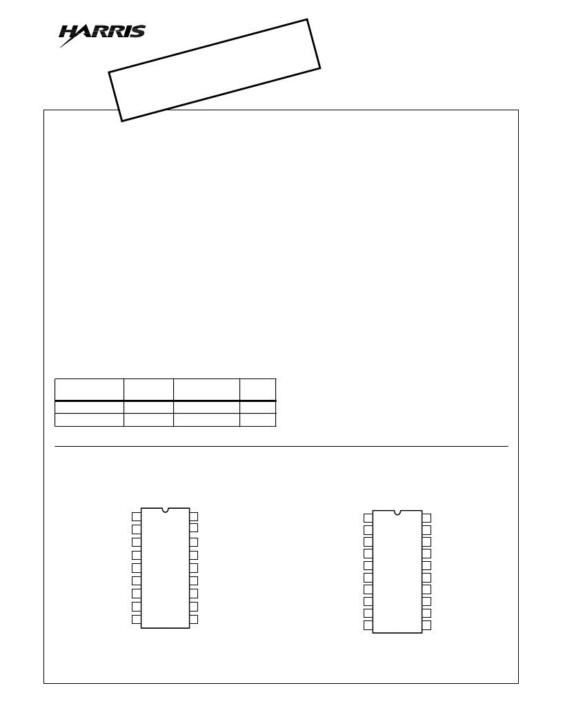
Pinouts
Part Number Information
PART NUMBER
TEMP.
RANGE (
o
C)
PACKAGE
PKG.
NO.
CA3256E
-40 to 85
18 Ld PDIP
E18.3
CA3256M
-40 to 85
20 Ld SOIC
M20.3
CA3256
(PDIP)
TOP VIEW
CA3256
(SOIC)
TOP VIEW
10
11
12
13
14
15
16
17
18
9
8
7
6
5
4
3
2
1
CONTROL B
CONTROL A
IN 1
IN/OUT 5
LED 1
LED 2
IN 2
LED 3
IN 3
LED 4
IN 4
GND
ENABLE
FEEDBACK
CONTROL C
AMP OUT
V-
V+
11
12
13
14
15
16
17
18
20
19
10
9
8
7
6
5
4
3
2
1
IN3
LED4
IN4
GND
V-
ENABLE
FEEDBACK
CONTROL C
AMP OUT
LED3
CONTROL B
CONTROL A
NC
IN1
IN2
V+
IN/OUT5
NC
LED1
LED2
[ /Title
(CA32
56)
/Sub-
ject
(25MH
z,
BiMO
S Ana-
log
Video
Switch
and
Ampli-
fier)
/Autho
r ()
/Key-
words
(Har-
ris
Semi-
con-
ductor,
4x1,
video
cross-
point
switch,
multi-
plexer
multi-
plexor,
cable
driver,
5x1,
moni
tor out-
put,
adjust-
able
gain,
NO REOBSOLETE PRODUCT
Call or email: centapp@harris.com
相關(guān)PDF資料 |
PDF描述 |
|---|---|
| CA3256E | 25MHz, BiMOS Analog Video Switch and Amplifier |
| CA3256M | 25MHz, BiMOS Analog Video Switch and Amplifier |
| CA3260AEZ | 4MHz, BiMOS Operational Amplifier with MOSFET Input/CMOS Output |
| CA3260EZ | 4MHz, BiMOS Operational Amplifier with MOSFET Input/CMOS Output |
| CA3260 | 4MHz, BiMOS Operational Amplifier with MOSFET Input/CMOS Output |
相關(guān)代理商/技術(shù)參數(shù) |
參數(shù)描述 |
|---|---|
| CA3256 WAF | 制造商:Harris Corporation 功能描述: |
| CA3256E | 制造商:Rochester Electronics LLC 功能描述:- Bulk |
| CA3256M | 制造商:Rochester Electronics LLC 功能描述:- Bulk |
| CA3256M96 | 制造商:未知廠家 制造商全稱:未知廠家 功能描述:Single Video Amplifier |
| CA3257E | 制造商:未知廠家 制造商全稱:未知廠家 功能描述:Consumer IC |
發(fā)布緊急采購,3分鐘左右您將得到回復。