- 您現在的位置:買賣IC網 > PDF目錄257668 > CD-700KAFHDB-12.000 (VECTRON INTERNATIONAL) PHASE LOCKED LOOP, CQCC16 PDF資料下載
參數資料
| 型號: | CD-700KAFHDB-12.000 |
| 廠商: | VECTRON INTERNATIONAL |
| 元件分類: | XO, clock |
| 英文描述: | PHASE LOCKED LOOP, CQCC16 |
| 封裝: | HERMETIC SEALED, CERAMIC, SMD-16 |
| 文件頁數: | 9/14頁 |
| 文件大小: | 146K |
| 代理商: | CD-700KAFHDB-12.000 |
CD-700, VCXO Based PLL
Vectron International
166 Glover Avenue, Norwalk, CT 06856 Tel: 1-88-VECTRON-1 http://www.vectron.com
CD-700 Theory of Operation
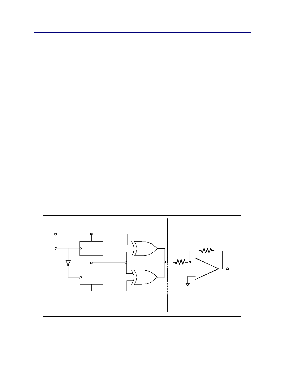
Phase Detector
The phase detector has two buffered inputs (DATAIN and CLKIN) which are designed to switch at
1.4 volts. DATAIN is designed to accept an NRZ data stream but may also be used for clock signals which
have a 50% duty cycle. CLKIN is connected to OUT1 or OUT2, or a divided version of one of these
outputs. CLKIN and DATAIN and are protected by ESD diodes and should not exceed the power supply
voltage or ground by more than a few hundred millivolts.
The phase detector is basically a latched flip flop/exclusive-or gate/differential amplifier filter design to
produce a DC signal proportional to the phase between the CLKIN and DATAIN signals (see Figure 4 for
a block diagram and Figure 5 for an open loop transfer curve). This will simplify the PLL design as the
designer does not have to filter narrow pulse signals to a DC level. Under locked conditions the rising
edge of CLKIN will be centered in the middle of the DATAIN signal (see Figure 6).
The phase detector gain is 0.53V/rad x data density for 5volt operation and 0.35V/rad x data density for
3.3 volt operation. Data density is equal to 1.0 for clock signals and is system dependent on coding and
design for NRZ signals, but 0.25 could be used as a starting point for data density.
The phase detector output is a DC signal for DATAIN frequencies greater than 1 MHz but produces
significant ripple when inputs are less than 200 kHz. Additional filtering is required for lower input
frequencies applications such as 8kHz (see Figures 8 and 9 as examples).
Under closed loop conditions the active filter has a blocking capacitor which provides a very high DC gain,
so under normal locked conditions and input frequencies >1 MHz, PHO will be about V
DD/2 and will not
vary significantly with changes in input frequency (within lock range). The control voltage (pin 16) will vary
according to the input frequency offset, but PHO will remain relatively constant.
D
Q1
Q2
D
Gain = 2 / 3
Gain = VDD / 2
π
30 k
20 k
PHO
(pin 3)
Clock In
(pin 6)
Data In
(pin 5)
Figure 4. Simplified Phase Detector Block Diagram
相關PDF資料 |
PDF描述 |
|---|---|
| CD-700KAFHGB-38.880 | PHASE LOCKED LOOP, CQCC16 |
| CD-700KAFNAB-16.384 | PHASE LOCKED LOOP, CQCC16 |
| CD-700KAFNAB-40.960 | PHASE LOCKED LOOP, CQCC16 |
| CD-700KAFNCB-49.152 | PHASE LOCKED LOOP, CQCC16 |
| CD-700KAFNFB-44.736 | PHASE LOCKED LOOP, CQCC16 |
相關代理商/技術參數 |
參數描述 |
|---|---|
| CD-700-KAF-HDB-13.000 | 制造商:未知廠家 制造商全稱:未知廠家 功能描述:Phase-Locked Loop |
| CD-700-KAF-HDB-16.000 | 制造商:未知廠家 制造商全稱:未知廠家 功能描述:Phase-Locked Loop |
| CD-700-KAF-HDB-16.384 | 制造商:未知廠家 制造商全稱:未知廠家 功能描述:Phase-Locked Loop |
| CD-700-KAF-HDB-19.440 | 制造商:未知廠家 制造商全稱:未知廠家 功能描述:Phase-Locked Loop |
| CD-700-KAF-HDB-20.000 | 制造商:未知廠家 制造商全稱:未知廠家 功能描述:Phase-Locked Loop |
發布緊急采購,3分鐘左右您將得到回復。