- 您現(xiàn)在的位置:買賣IC網(wǎng) > PDF目錄379897 > CLC5526PCASM (National Semiconductor Corporation) Digital Variable Gain Amplifier (DVGA) PDF資料下載
參數(shù)資料
| 型號: | CLC5526PCASM |
| 廠商: | National Semiconductor Corporation |
| 英文描述: | Digital Variable Gain Amplifier (DVGA) |
| 中文描述: | 數(shù)字可變增益放大器(DVGA) |
| 文件頁數(shù): | 1/10頁 |
| 文件大小: | 274K |
| 代理商: | CLC5526PCASM |
CLC5526
Digital Variable Gain Amplifier (DVGA)
General Description
The CLC5526 is a high performance, digitally controlled,
variable-gain amplifier (DVGA). It has been designed for use
in a broad range of mixed signal and digital communication
applications such as mobile radio, cellular base stations and
back-channel modems where automatic-gain-control (AGC)
is required to increase system dynamic range.
The CLC5526 has differential input and output, allowing
large signal swings on a single 5V rail. The input impedance
is 200
. The differential output impedance is 600
and is
designed to drive a 1 k
differential load. The output ampli-
fier
has
excellent
intermodulation
CLC5526 is designed to accept signals from RF elements
and maintain a terminated impedance environment.
The CLC5526 maintains a 350 MHz bandwidth over its en-
tire gain and attenuation range from +30 dB to 12 dB. Inter-
nal clamping ensures very fast overdrive recovery. Two tone
intermodulation distortion is excellent: at 150 MHz, 1 V
pp
it is
64 dBc.
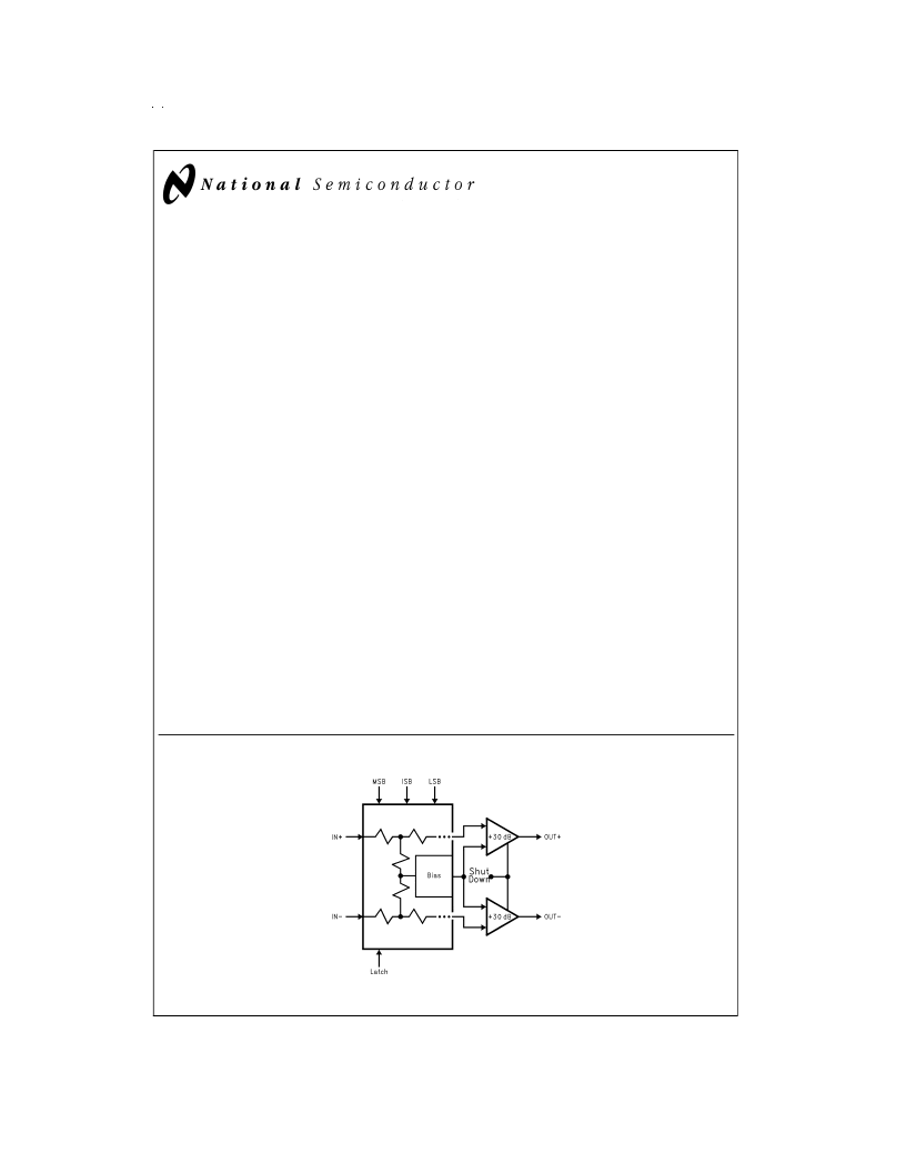
Input signals to the CLC5526 are scaled by an accurate, dif-
ferential R-2R resistive ladder with an input impedance of
200
. A scaled version of the input is selected under digital
control and passed to the internal amplifier. The input com-
mon mode level is set at 2.4V via a bandgap referenced bias
generator which can be overridden by an external input.
Following the resistive ladder is a fixed, 30 dB gain amplifier.
The output stage common mode voltage of the CLC5526 is
set to 3V, by internal, positive supply connected resistors.
Digital control of the CLC5526 is accomplished by a 3-bit
parallel gain control input and a data valid pin to latch the
data. If the data is not latched, the DVGA is transparent to
gain control updates. All digital inputs are TTL/CMOS com-
patible.
performance.
The
A shutdown input reduces the CLC5526 supply currrent to a
few mA. During shutdown, the input termination is main-
tained and current attenuation settings are held.
The CLC5526 operates over the industrial temperature
range of 40C to +85C. The part is available in a 20-pin
SSOP package.
Features
n
350 MHz bandwidth
n
Differential input and output
n
Gain control: parallel w/data latching
n
Supply voltage:
n
Supply current:
+5V
48 mA
Key Specifications
n
Low two tone intermod:
distortion: 64 dBc
@
1 V
PP
, 150 MHz
24.5 dBm IP3, 150 MHz
n
Low noise:
2.5 nV/
√
Hz (max gain),
9.3 dB noise figure (max gain)
n
Wide gain range:
n
Gain step size:
6 dB
+30 dB to 12 dB
Applications
n
Cellular/PCS base stations
n
IF sampling receivers
n
Infrared/CCD imaging
n
Back-channel modems
n
Electro-optics
n
Instrumentation
n
Medical imaging
n
High definition video
Block Diagram
DS015016-2
June 1999
C
1999 National Semiconductor Corporation
DS015016
www.national.com
相關(guān)PDF資料 |
PDF描述 |
|---|---|
| CLC5526 | Digital Variable Gain Amplifier (DVGA) |
| CLC5526MSA | Digital Variable Gain Amplifier (DVGA) |
| CLC5602 | Dual, High Output, Video Amplifier |
| CLC5602IM | Dual, High Output, Video Amplifier |
| CLC5602IMX | Dual, High Output, Video Amplifier |
相關(guān)代理商/技術(shù)參數(shù) |
參數(shù)描述 |
|---|---|
| CLC5602 | 制造商:NSC 制造商全稱:National Semiconductor 功能描述:Dual, High Output, Video Amplifier |
| CLC5602IM | 制造商:OC White Company 功能描述:OP Amp Dual Current Fdbk 8-Pin SOIC N |
| CLC5602IMX | 制造商:Rochester Electronics LLC 功能描述:- Bulk |
| CLC5602IN | 制造商:Rochester Electronics LLC 功能描述:- Bulk |
| CLC5602M/N WAF | 制造商:Texas Instruments 功能描述: |
發(fā)布緊急采購,3分鐘左右您將得到回復(fù)。