- 您現在的位置:買賣IC網 > PDF目錄357723 > CY62146V18-85BAI x16 SRAM PDF資料下載
參數資料
| 型號: | CY62146V18-85BAI |
| 英文描述: | x16 SRAM |
| 中文描述: | x16的SRAM |
| 文件頁數: | 1/10頁 |
| 文件大小: | 153K |
| 代理商: | CY62146V18-85BAI |
256K x 16 Static RAM
CY62147V18 MoBL2
Cypress Semiconductor Corporation
3901 North First Street
San Jose
CA 95134
408-943-2600
September 6, 2000
Features
Low voltage range:
—CY62147V18: 1.75V–1.95V
Ultra-low active, standby power
Easy memory expansion with CE and OE features
TTL-compatible inputs and outputs
Automatic power-down when deselected
CMOS for optimum speed/power
Functional Description
The CY62147V18 is a high-performance CMOS static RAM
organized as 262,144 words by 16 bits. These devices feature
advanced circuit design to provide ultra-low active current.
This is ideal for providing More Battery Life (MoBL) in por-
table applications such as cellular telephones. The devices
also have an automatic power-down feature that significantly
reduces power consumption by 99% when addresses are not
toggling. The device can also be put into standby mode when
deselected (CE HIGH) or when CE is LOW and both BLE and
BHE are HIGH. The input/output pins (I/O
0
through I/O
15
) are
placed in a high-impedance state when: deselected (CE
HIGH), outputs are disabled (OE HIGH), BHE and BLE are
disabled (BHE, BLE HIGH), or during a write operation (CE
LOW, and WE LOW).
Writing to the device is accomplished by taking Chip Enable
(CE) and Write Enable (WE) inputs LOW. If Byte Low Enable
(BLE) is LOW, then data from I/O pins (I/O
0
through I/O
7
), is
written into the location specified on the address pins (A
0
through A
17
). If Byte High Enable (BHE) is LOW, then data
from I/O pins (I/O
8
through I/O
15
) is written into the location
specified on the address pins (A
0
through A
17
).
Reading from the device is accomplished by taking Chip
Enable (CE) and Output Enable (OE) LOW while forcing the
Write Enable (WE) HIGH. If Byte Low Enable (BLE) is LOW,
then data from the memory location specified by the address
pins will appear on I/O
0
to I/O
7
. If Byte High Enable (BHE) is
LOW, then data from memory will appear on I/O
8
to I/O
15
. See
the truth table at the back of this data sheet for a complete
description of read and write modes.
The CY62147V18 is available in 48-ball FBGA packaging.
MoBL2 and More Battery Life are trademarks of Cypress Semiconductor Corporation.
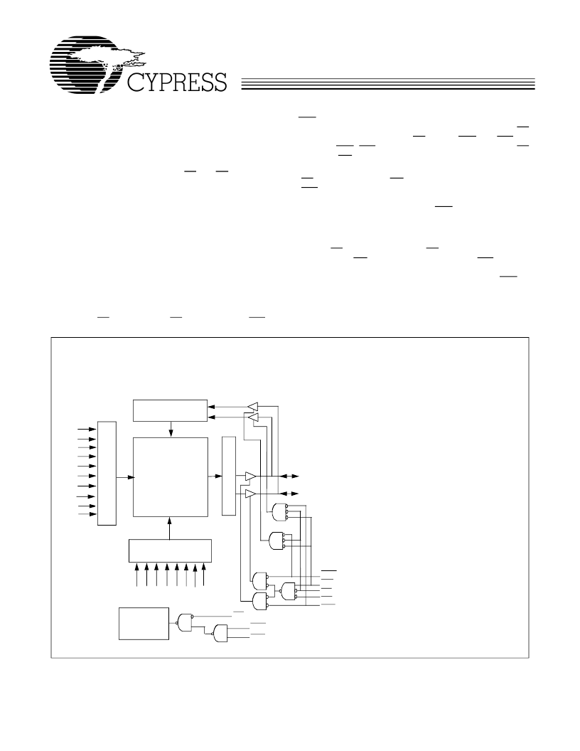
Logic Block Diagram
256K x 16
RAM Array
2048 x 2048
I/O
0
– I/O
7
R
A
8
A
7
A
6
A
5
A
4
A
3
A
2
A
1
COLUMN DECODER
A
1
A
1
A
1
A
1
A
1
S
DATA IN DRIVERS
OE
BLE
I/O
8
– I/O
15
CE
WE
BHE
A
1
A
1
A
0
A
1
A
9
Power
-
Down
Circuit
BHE
BLE
CE
相關PDF資料 |
PDF描述 |
|---|---|
| CY62146V18LL-70BAI | x16 SRAM |
| CY62147V18LL-70BAI | x16 SRAM |
| CY62147VLL-70BAI | SRAM|256KX16|CMOS|BGA|48PIN|PLASTIC |
| CY62148-100SC | x8 SRAM |
| CY62148-100SI | x8 SRAM |
相關代理商/技術參數 |
參數描述 |
|---|---|
| CY62146V18LL-70BAI | 制造商:未知廠家 制造商全稱:未知廠家 功能描述:x16 SRAM |
| CY62146VLL-70BAI | 制造商:Cypress Semiconductor 功能描述:SRAM Chip Async Single 3V 4M-Bit 256K x 16 70ns 48-Pin FBGA 制造商:Rochester Electronics LLC 功能描述:4MB (256K X 16)- SLOW ASYNCH SRAM - Bulk |
| CY62146VLL-70BAIT | 制造商:Cypress Semiconductor 功能描述:SRAM Chip Async Single 3V 4M-Bit 256K x 16 70ns 48-Pin FBGA T/R |
| CY62146VLL-70ZI | 制造商:Cypress Semiconductor 功能描述: |
| CY62146VLL-70ZS1 | 制造商:Cypress Semiconductor 功能描述: |
發布緊急采購,3分鐘左右您將得到回復。