- 您現在的位置:買賣IC網 > PDF目錄298975 > CY7C1328F-133AC (CYPRESS SEMICONDUCTOR CORP) 256K X 18 CACHE SRAM, 4 ns, PQFP100 PDF資料下載
參數資料
| 型號: | CY7C1328F-133AC |
| 廠商: | CYPRESS SEMICONDUCTOR CORP |
| 元件分類: | SRAM |
| 英文描述: | 256K X 18 CACHE SRAM, 4 ns, PQFP100 |
| 封裝: | 14 X 20 MM, 1.40 MM HEIGHT, PLASTIC, TQFP-100 |
| 文件頁數: | 1/17頁 |
| 文件大小: | 353K |
| 代理商: | CY7C1328F-133AC |
4-Mb (256K x 18) Pipelined DCD Sync SRAM
CY7C1328F
Cypress Semiconductor Corporation
3901 North First Street
San Jose
, CA 95134
408-943-2600
Document #: 38-05220 Rev. *A
Revised January 19, 2004
Features
Registered inputs and outputs for pipelined operation
Optimal for performance (Double-Cycle deselect)
— Depth expansion without wait state
256K × 18-bit common I/O architecture
3.3V –5% and +10% core power supply (VDD)
3.3V / 2.5V I/O supply (VDDQ)
Fast clock-to-output times
— 2.6 ns (for 250-MHz device)
— 2.6 ns (for 225-MHz device)
— 2.8 ns (for 200-MHz device)
— 3.5 ns (for 166-MHz device)
— 4.0 ns (for 133-MHz device)
— 4.5 ns (for 100-MHz device)
Provide high-performance 3-1-1-1 access rate
User-selectable burst counter supporting Intel
Pentium interleaved or linear burst sequences
Separate processor and controller address strobes
Synchronous self-timed writes
Asynchronous Output Enable
JEDEC-standard 100-pin TQFP package and pinout
“ZZ” Sleep Mode option
Functional Description[1]
The CY7C1328F SRAM integrates 262,144 x 18 SRAM cells
with advanced synchronous peripheral circuitry and a two-bit
counter for internal burst operation. All synchronous inputs are
gated by registers controlled by a positive-edge-triggered
Clock Input (CLK). The synchronous inputs include all
addresses, all data inputs, address-pipelining Chip Enable
(CE1), depth-expansion Chip Enables (CE2 and CE3), Burst
Control inputs (ADSC, ADSP, and ADV), Write Enables
(BW[A:B], and BWE), and Global Write (GW). Asynchronous
inputs include the Output Enable (OE) and the ZZ pin.
Addresses and chip enables are registered at rising edge of
clock when either Address Strobe Processor (ADSP) or
Address Strobe Controller (ADSC) are active. Subsequent
burst addresses can be internally generated as controlled by
the Advance pin (ADV).
Address, data inputs, and write controls are registered on-chip
to initiate a self-timed Write cycle.This part supports Byte Write
operations (see Pin Descriptions and Truth Table for further
details). Write cycles can be one to two bytes wide as
controlled by the byte write control inputs. GW active LOW
causes all bytes to be written. This device incorporates an
additional pipelined enable register which delays turning off
the output buffers an additional cycle when a deselect is
executed.This feature allows depth expansion without penal-
izing system performance.
The CY7C1328F operates from a +3.3V core power supply
while all outputs operate with a +3.3V or a +2.5V supply. All
inputs and outputs are JEDEC-standard JESD8-5-compatible.
Note:
1. For best-practices recommendations, please refer to the Cypress application note System Design Guidelines on www.cypress.com.
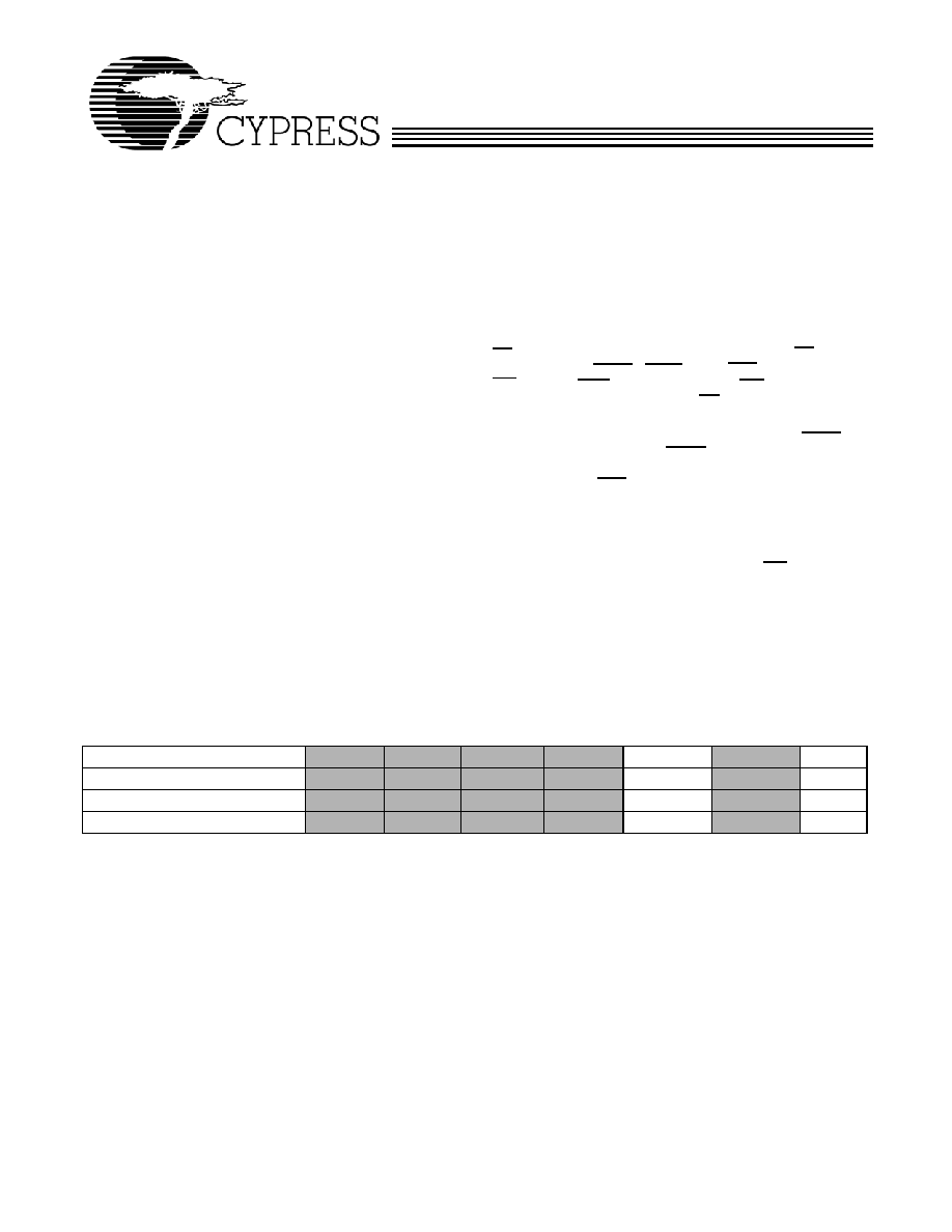
Selection Guide
250 MHz
225 MHz
200 MHz
166 MHz
133 MHz
100 MHz
Unit
Maximum Access Time
2.6
2.8
3.5
4.0
4.5
ns
Maximum Operating Current
325
290
265
240
225
205
mA
Maximum CMOS Standby Current
40
mA
Shaded areas contain advance information.
Please contact your local Cypress sales representative for availability of these parts.
相關PDF資料 |
PDF描述 |
|---|---|
| CY7C1339B-133BGIT | 128K X 32 CACHE SRAM, 4 ns, PBGA119 |
| CY7C1339G-200AXCT | 128K X 32 CACHE SRAM, 2.8 ns, PQFP100 |
| CY7C1347D-250BGC | 128K X 36 CACHE SRAM, 2.4 ns, PBGA119 |
| CY7C1512JV18-267BZXC | 4M X 18 QDR SRAM, 0.45 ns, PBGA165 |
| CY7C1515AV18-250BZXI | 2M X 36 QDR SRAM, 0.45 ns, PBGA165 |
相關代理商/技術參數 |
參數描述 |
|---|---|
| CY7C1328F-200AC | 制造商:Cypress Semiconductor 功能描述:SRAM Chip Sync Dual 3.3V 4.5M-Bit 256K x 18 2.8ns 100-Pin TQFP |
| CY7C1328G-133AXI | 功能描述:靜態隨機存取存儲器 256Kx18 3.3V IND Sync FT 靜態隨機存取存儲器 RoHS:否 制造商:Cypress Semiconductor 存儲容量:16 Mbit 組織:1 M x 16 訪問時間:55 ns 電源電壓-最大:3.6 V 電源電壓-最小:2.2 V 最大工作電流:22 uA 最大工作溫度:+ 85 C 最小工作溫度:- 40 C 安裝風格:SMD/SMT 封裝 / 箱體:TSOP-48 封裝:Tray |
| CY7C1328G-133AXIT | 功能描述:靜態隨機存取存儲器 256Kx18 3.3V IND Sync FT 靜態隨機存取存儲器 RoHS:否 制造商:Cypress Semiconductor 存儲容量:16 Mbit 組織:1 M x 16 訪問時間:55 ns 電源電壓-最大:3.6 V 電源電壓-最小:2.2 V 最大工作電流:22 uA 最大工作溫度:+ 85 C 最小工作溫度:- 40 C 安裝風格:SMD/SMT 封裝 / 箱體:TSOP-48 封裝:Tray |
| CY7C1328G-250AXC | 功能描述:靜態隨機存取存儲器 256Kx18 3.3V COM Sync FT 靜態隨機存取存儲器 RoHS:否 制造商:Cypress Semiconductor 存儲容量:16 Mbit 組織:1 M x 16 訪問時間:55 ns 電源電壓-最大:3.6 V 電源電壓-最小:2.2 V 最大工作電流:22 uA 最大工作溫度:+ 85 C 最小工作溫度:- 40 C 安裝風格:SMD/SMT 封裝 / 箱體:TSOP-48 封裝:Tray |
| CY7C1328G-250AXCT | 功能描述:靜態隨機存取存儲器 256Kx18 3.3V COM Sync FT 靜態隨機存取存儲器 RoHS:否 制造商:Cypress Semiconductor 存儲容量:16 Mbit 組織:1 M x 16 訪問時間:55 ns 電源電壓-最大:3.6 V 電源電壓-最小:2.2 V 最大工作電流:22 uA 最大工作溫度:+ 85 C 最小工作溫度:- 40 C 安裝風格:SMD/SMT 封裝 / 箱體:TSOP-48 封裝:Tray |
發布緊急采購,3分鐘左右您將得到回復。