- 您現(xiàn)在的位置:買賣IC網(wǎng) > PDF目錄352947 > CY7C199-15LC x8 SRAM PDF資料下載
參數(shù)資料
| 型號(hào): | CY7C199-15LC |
| 英文描述: | x8 SRAM |
| 中文描述: | x8的SRAM |
| 文件頁(yè)數(shù): | 1/9頁(yè) |
| 文件大小: | 194K |
| 代理商: | CY7C199-15LC |
128K x 8 Static RAM
CY7C1019B/
CY7C10191B
Cypress Semiconductor Corporation
3901 North First Street
San Jose
CA 95134
408-943-2600
Document #: 38-05026 Rev. *A
Revised August 13, 2002
C1019V33
Features
High speed
—tAA = 10, 12, 15 ns
CMOS for optimum speed/power
Center power/ground pinout
Automatic power-down when deselected
Easy memory expansion with CE and OE options
Functionally equivalent to CY7C1019
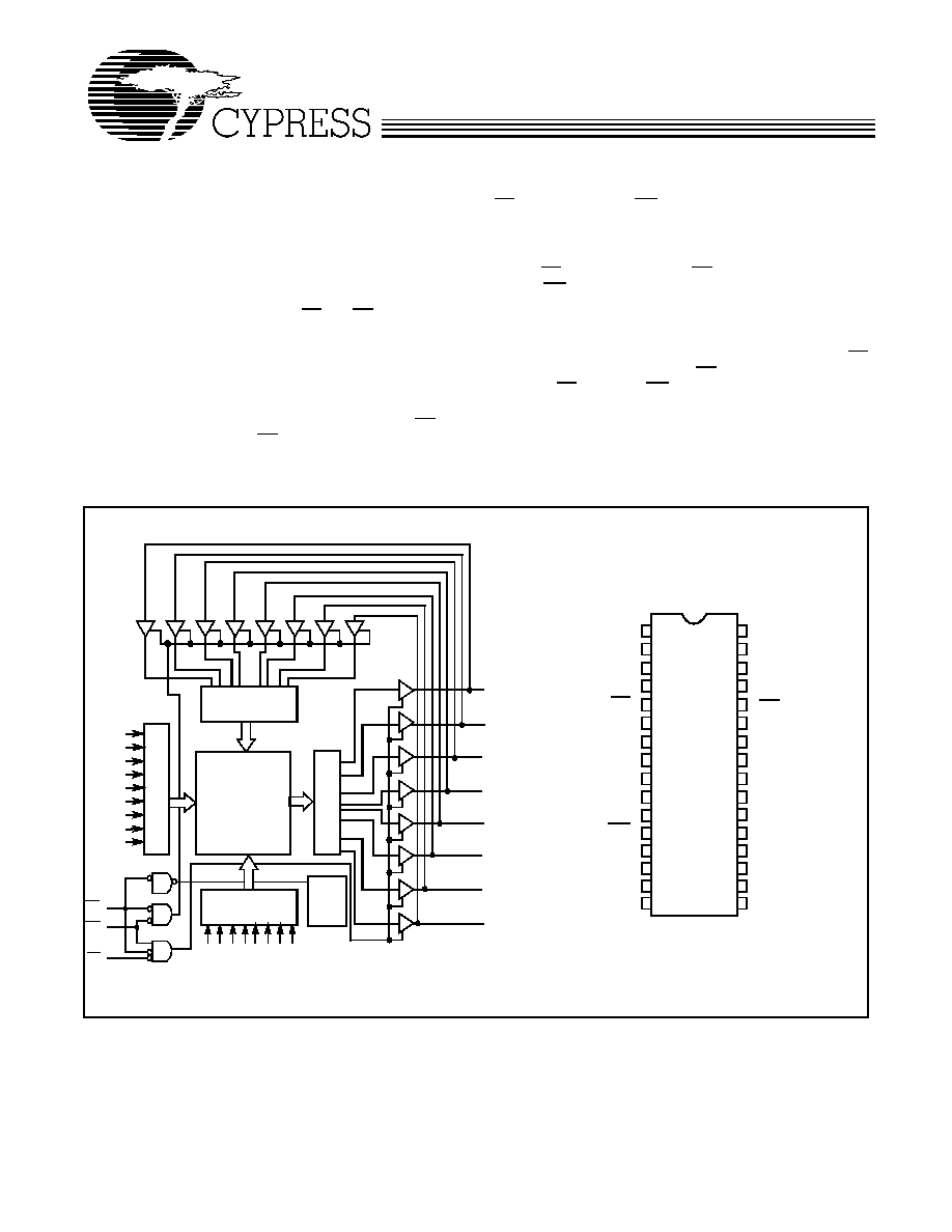
Functional Description
The CY7C1019B/10191B is a high-performance CMOS static
RAM organized as 131,072 words by 8 bits. Easy memory
expansion is provided by an active LOW Chip Enable (CE), an
active LOW Output Enable (OE), and three-state drivers. This
device has an automatic power-down feature that significantly
reduces power consumption when deselected.
Writing to the device is accomplished by taking Chip Enable
(CE) and Write Enable (WE) inputs LOW. Data on the eight I/O
pins (I/O0 through I/O7) is then written into the location speci-
fied on the address pins (A0 through A16).
Reading from the device is accomplished by taking Chip
Enable (CE) and Output Enable (OE) LOW while forcing Write
Enable (WE) HIGH. Under these conditions, the contents of
the memory location specified by the address pins will appear
on the I/O pins.
The eight input/output pins (I/O0 through I/O7) are placed in a
high-impedance state when the device is deselected (CE
HIGH), the outputs are disabled (OE HIGH), or during a write
operation (CE LOW, and WE LOW).
The CY7C1019B/10191B is available in standard 32-pin
TSOP Type II and 400-mil-wide SOJ packages. Customers
should use part number CY7C10191B when ordering parts
with 10 ns tAA, and CY7C1019B when ordering 12 and 15 ns
tAA.
14
15
ogic Block Diagram
Pin Configurations
A1
A2
A3
A4
A5
A6
A7
A8
COLUMN
DECODER
ROW
DEC
O
D
E
R
SE
NSE
A
M
PS
INPUT BUFFER
POWER
DOWN
WE
OE
I/O0
I/O1
I/O2
I/O3
512 x 256 x 8
ARRAY
I/O7
I/O6
I/O5
I/O4
A0
A
11
A
13
A
12
A
10
CE
A
16
A
9
1
2
3
4
5
6
7
8
9
10
11
14
19
20
24
23
22
21
25
28
27
26
Top View
SOJ
12
13
29
32
31
30
16
15
17
18
A7
A1
A2
A3
CE
I/O0
I/O1
VCC
A13
A16
A15
OE
I/O7
I/O6
A12
A11
A10
A9
I/O2
A0
A4
A5
A6
I/O4
VCC
I/O5
A8
I/O3
WE
VSS
A14
V
SS
/ TSOPII
相關(guān)PDF資料 |
PDF描述 |
|---|---|
| CY7C199-15VCT | x8 SRAM |
| CY7C199-15VIT | x8 SRAM |
| CY7C199-20DC | x8 SRAM |
| CY7C199-20KMB | x8 SRAM |
| CY7C199-20LC | x8 SRAM |
相關(guān)代理商/技術(shù)參數(shù) |
參數(shù)描述 |
|---|---|
| CY7C19915PC | 制造商:CYPRESS 功能描述:7C199-15PC |
| CY7C199-15PC | 功能描述:IC SRAM 256KBIT 15NS 28DIP RoHS:否 類別:集成電路 (IC) >> 存儲(chǔ)器 系列:- 標(biāo)準(zhǔn)包裝:96 系列:- 格式 - 存儲(chǔ)器:閃存 存儲(chǔ)器類型:FLASH 存儲(chǔ)容量:16M(2M x 8,1M x 16) 速度:70ns 接口:并聯(lián) 電源電壓:2.65 V ~ 3.6 V 工作溫度:-40°C ~ 85°C 封裝/外殼:48-TFSOP(0.724",18.40mm 寬) 供應(yīng)商設(shè)備封裝:48-TSOP 包裝:托盤 |
| CY7C199-15VC | 功能描述:IC SRAM 256KBIT 15NS 28SOJ RoHS:否 類別:集成電路 (IC) >> 存儲(chǔ)器 系列:- 標(biāo)準(zhǔn)包裝:96 系列:- 格式 - 存儲(chǔ)器:閃存 存儲(chǔ)器類型:FLASH 存儲(chǔ)容量:16M(2M x 8,1M x 16) 速度:70ns 接口:并聯(lián) 電源電壓:2.65 V ~ 3.6 V 工作溫度:-40°C ~ 85°C 封裝/外殼:48-TFSOP(0.724",18.40mm 寬) 供應(yīng)商設(shè)備封裝:48-TSOP 包裝:托盤 |
| CY7C19915VCT | 制造商:CYPRESS 功能描述:* |
| CY7C199-15VCT | 制造商:Cypress Semiconductor 功能描述:SRAM Chip Async Single 5V 256K-Bit 32K x 8 15ns 28-Pin SOJ T/R |
發(fā)布緊急采購(gòu),3分鐘左右您將得到回復(fù)。