- 您現在的位置:買賣IC網 > PDF目錄19022 > DC1369A-G (Linear Technology)BOARD DEMO 125MSPS LTC2261-12 PDF資料下載
參數資料
| 型號: | DC1369A-G |
| 廠商: | Linear Technology |
| 文件頁數: | 18/34頁 |
| 文件大小: | 0K |
| 描述: | BOARD DEMO 125MSPS LTC2261-12 |
| 軟件下載: | QuikEval II System |
| 設計資源: | DC1369A Design Files |
| 標準包裝: | 1 |
| 系列: | * |
| 相關產品: | DC890B-ND - BOARD USB DATA COLLECTION |
第1頁第2頁第3頁第4頁第5頁第6頁第7頁第8頁第9頁第10頁第11頁第12頁第13頁第14頁第15頁第16頁第17頁當前第18頁第19頁第20頁第21頁第22頁第23頁第24頁第25頁第26頁第27頁第28頁第29頁第30頁第31頁第32頁第33頁第34頁
LTC2261-12
LTC2260-12/LTC2259-12
25
226112fc
For more information www.linear.com/LTC2261-12
The digital output is decoded at the receiver by inverting
the odd bits (D1, D3, D5, D7, D9, D11). The alternate
bit polarity mode is independent of the digital output
randomizer—either, both or neither function can be on
at the same time. When alternate bit polarity mode is on,
the data format is offset binary and the 2’s complement
control bit has no effect. The alternate bit polarity mode is
enabledbyseriallyprogrammingmodecontrolregisterA4.
Digital Output Test Patterns
To allow in-circuit testing of the digital interface to the
A/D, there are several test modes that force the A/D data
outputs (OF, D11-D0) to known values:
All 1s: All outputs are 1
All 0s: All outputs are 0
Alternating: Outputs change from all 1s to all 0s on
alternating samples
Checkerboard: Outputs change from 1010101010101
to 0101010101010 on alternating samples
The digital output test patterns are enabled by serially
programming mode control register A4. When enabled,
the test patterns override all other formatting modes: 2’s
complement, randomizer, alternate-bit-polarity.
Output Disable
The digital outputs may be disabled by serially program-
mingmodecontrolregisterA3.Alldigitaloutputsincluding
OFandCLKOUTaredisabled.Thehighimpedancedisabled
state is intended for long periods of inactivity—it is too
slow to multiplex a data bus between multiple converters
at full speed.
Sleep and Nap Modes
The A/D may be placed in sleep or nap modes to conserve
power. In sleep mode the entire A/D converter is powered
down,resultingin0.5mWpowerconsumption.Sleepmode
is enabled by mode control register A1 (serial program-
ming mode), or by SDI (parallel programming mode).
The amount of time required to recover from sleep mode
depends on the size of the bypass capacitors on VREF,
REFH, and REFL. For the suggested values in Figure 8,
the A/D will stabilize after 2ms.
InnapmodetheA/Dcoreispowereddownwhiletheinternal
referencecircuitsstayactive,allowingfasterwake-upthan
from sleep mode. Recovering from nap mode requires at
least 100 clock cycles. If the application demands very
accurate DC settling then an additional 50s should be
allowedsotheon-chipreferencescansettlefromtheslight
temperature shift caused by the change in supply current
as the A/D leaves nap mode. Nap mode is enabled by mode
control register A1 in the serial programming mode.
DEVICE PROGRAMMING MODES
The operating modes of the LTC2261-12 can be pro-
grammed by either a parallel interface or a simple serial
interface. The serial interface has more flexibility and
can program all available modes. The parallel interface
is more limited and can only program some of the more
commonly used modes.
Parallel Programming Mode
To use the parallel programming mode, PAR/SER should
be tied to VDD. The CS, SCK and SDI pins are binary logic
inputs that set certain operating modes. These pins can
be tied to VDD or ground, or driven by 1.8V, 2.5V or 3.3V
CMOS logic. Table 2 shows the modes set by CS, SCK
and SDI.
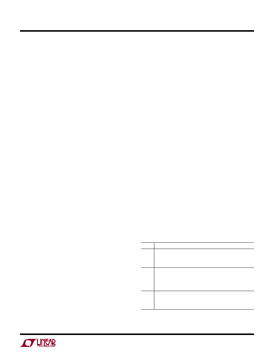
Table 2. Parallel Programming Mode Control Bits (PAR/SER = VDD)
PIN
DESCRIPTION
CS
Clock Duty Cycle Stabilizer Control Bit
0 = Clock Duty Cycle Stabilizer Off
1 = Clock Duty Cycle Stabilizer On
SCK
Digital Output Mode Control Bit
0 = Full-Rate CMOS Output Mode
1 = Double-Data Rate LVDS Output Mode
(3.5mA LVDS Current, Internal Termination Off)
SDI
Power Down Control Bit
0 = Normal Operation
1 = Sleep Mode
applicaTions inForMaTion
相關PDF資料 |
PDF描述 |
|---|---|
| 8097 | T-1 12V .050" BI-PIN BASE |
| A3CT-7021 | SWITCH UNIT-IP40 |
| A3CJ-7121 | SWITCH UNIT-IP40 |
| KPR113 | LED KRYTON IND B3 1/2 4.8V MINI |
| DC1369A-A | BOARD DEMO 125MSPS LTC2261-14 |
相關代理商/技術參數 |
參數描述 |
|---|---|
| DC1369A-H | 功能描述:BOARD DEMO 105MSPS LTC2260-12 RoHS:是 類別:未定義的類別 >> 其它 系列:* 標準包裝:1 系列:* 其它名稱:MS305720A |
| DC1369A-I | 功能描述:BOARD DEMO 80MSPS LTC2259-12 RoHS:是 類別:未定義的類別 >> 其它 系列:* 標準包裝:1 系列:* 其它名稱:MS305720A |
| DC1369A-J | 制造商:Linear Technology 功能描述:12BIT ADC Eval Brd, Rq. DC1371 & DC1075 制造商:Linear Technology 功能描述:12BIT ADC Eval Brd, Rq. DC1371 & DC1075; Silicon Manufacturer:Linear Technology; Silicon Core Number:LTC2258-12; Kit Application Type:Data Converter; Application Sub Type:ADC; Kit Contents:Board, Guide |
| DC1369A-K | 制造商:Linear Technology 功能描述:12BIT ADC Eval Brd, Rq. DC1371 & DC1075 制造商:Linear Technology 功能描述:12BIT ADC Eval Brd, Rq. DC1371 & DC1075; Silicon Manufacturer:Linear Technology; Silicon Core Number:LTC2257-12; Kit Application Type:Data Converter; Application Sub Type:ADC; Kit Contents:Board, Guide |
| DC1369A-L | 制造商:Linear Technology 功能描述:12BIT ADC Eval Brd, Rq. DC1371 & DC1075 制造商:Linear Technology 功能描述:12BIT ADC Eval Brd, Rq. DC1371 & DC1075; Silicon Manufacturer:Linear Technology; Silicon Core Number:LTC2256-12; Kit Application Type:Data Converter; Application Sub Type:ADC; Kit Contents:Board, Guide |
發布緊急采購,3分鐘左右您將得到回復。