- 您現在的位置:買賣IC網 > PDF目錄19027 > DC1525A-E (Linear Technology)BOARD DEMO 40MSPS LTC2171-14 PDF資料下載
參數資料
| 型號: | DC1525A-E |
| 廠商: | Linear Technology |
| 文件頁數: | 18/34頁 |
| 文件大小: | 0K |
| 描述: | BOARD DEMO 40MSPS LTC2171-14 |
| 軟件下載: | QuikEval II System |
| 設計資源: | DC1525A Design Files |
| 標準包裝: | 1 |
| 系列: | * |
| 相關產品: | DC1371A-ND - BOARD USB DATA ACQUISITION HS |
第1頁第2頁第3頁第4頁第5頁第6頁第7頁第8頁第9頁第10頁第11頁第12頁第13頁第14頁第15頁第16頁第17頁當前第18頁第19頁第20頁第21頁第22頁第23頁第24頁第25頁第26頁第27頁第28頁第29頁第30頁第31頁第32頁第33頁第34頁
LTC2172-14/
LTC2171-14/LTC2170-14
25
21721014fb
applied—an exclusive-OR operation is applied between
the LSB and all other bits. The FR and DCO outputs are
not affected. The output randomizer is enabled by serially
programming mode control register A1.
Digital Output Test Pattern
To allow in-circuit testing of the digital interface to the
A/D, there is a test mode that forces the A/D data outputs
(D13-D0) of all channels to known values. The digital
output test patterns are enabled by serially programming
mode control registers A3 and A4. When enabled, the test
patterns override all other formatting modes: 2’s comple-
ment and randomizer.
Output Disable
The digital outputs may be disabled by serially program-
ming mode control register A2. The current drive for all
digital outputs, including DCO and FR, are disabled to save
powerorenablein-circuittesting.Whendisabled,thecom-
mon mode of each output pair becomes high impedance,
but the differential impedance may remain low.
Sleep and Nap Modes
The A/D may be placed in sleep or nap modes to conserve
power. In sleep mode the entire chip is powered down,
resulting in 1mW power consumption. Sleep mode is
enabled by mode control register A1 (serial program-
ming mode), or by SDI (parallel programming mode).
The amount of time required to recover from sleep mode
depends on the size of the bypass capacitors on VREF,
REFH and REFL. For the suggested values in Figure 8, the
A/D will stabilize after 2ms.
In nap mode any combination of A/D channels can be
powered down while the internal reference circuits and the
PLL stay active, allowing a faster wake-up than from sleep
mode. Recovering from nap mode requires at least 100
clock cycles. If the application demands very accurate DC
settling, then an additional 50s should be allowed so the
on-chip references can settle from the slight temperature
shift caused by the change in supply current as the A/D
leavesnapmode.Napmodeisenabledbythemodecontrol
register A1 in the serial programming mode.
applicaTions inForMaTion
DEVICE PROGRAMMING MODES
The operating modes of the LTC2172-14/LTC2171-14/
LTC2170-14 can be programmed by either a parallel
interface or a simple serial interface. The serial interface
has more flexibility and can program all available modes.
Theparallelinterfaceismorelimitedandcanonlyprogram
some of the more commonly used modes.
Parallel Programming Mode
To use the parallel programming mode, PAR/SER should
be tied to VDD. The CS, SCK, SDI and SDO pins are binary
logic inputs that set certain operating modes. These pins
can be tied to VDD or ground, or driven by 1.8V, 2.5V or
3.3V CMOS logic. When used as an input, SDO should
be driven through a 1k series resistor. Table 3 shows the
modes set by CS, SCK, SDI and SDO.
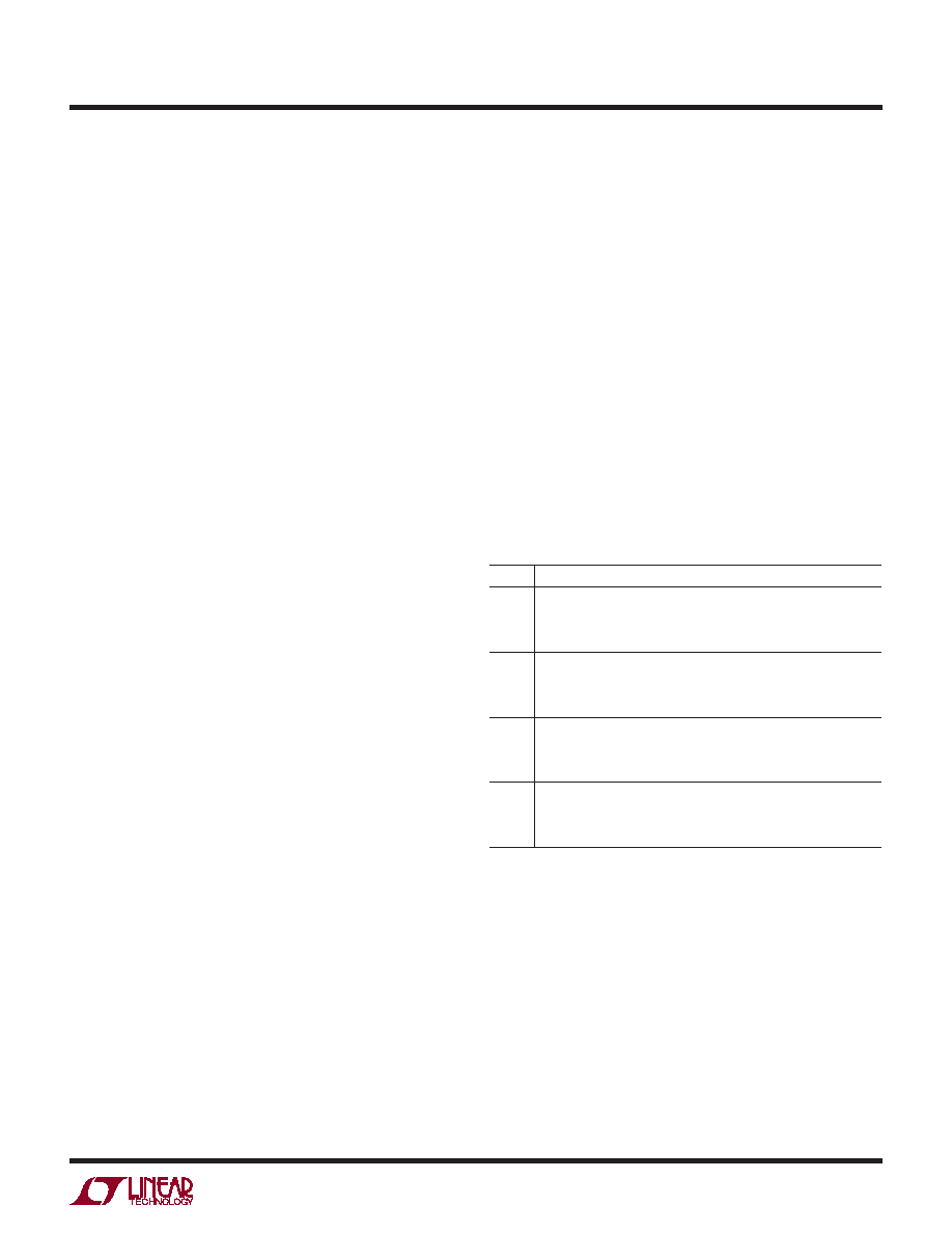
Table 3. Parallel Programming Mode Control Bits (PAR/SER = VDD)
PIN
DESCRIPTION
CS
2-Lane/1-Lane Selection Bit
0 = 2-Lane, 16-Bit Serialization Output Mode
1 = 1-Lane, 14-Bit Serialization Output Mode
SCK
LVDS Current Selection Bit
0 = 3.5mA LVDS Current Mode
1 = 1.75mA LVDS Current Mode
SDI
Power Down Control Bit
0 = Normal Operation
1 = Sleep Mode
SDO
Internal 100Ω Termination Selection Bit
0 = Internal Termination Disabled
1 = Internal Termination Enabled
Serial Programming Mode
To use the serial programming mode, PAR/SER should be
tied to ground. The CS, SCK, SDI and SDO pins become
a serial interface that program the A/D mode control
registers. Data is written to a register with a 16-bit serial
word. Data can also be read back from a register to verify
its contents.
Serial data transfer starts when CS is taken low. The data
on the SDI pin is latched at the first 16 rising edges of
SCK. Any SCK rising edges after the first 16 are ignored.
The data transfer ends when CS is taken high again.
相關PDF資料 |
PDF描述 |
|---|---|
| SM3620S | LAMP T-1.5 TELE SLIDE 36V .02A |
| VX-5-1A2 | SWITCH BASIC SPDT 5A .187QC |
| SM2850S | LAMP T-1.5 TELE SLIDE 28V .05A |
| SM2450S | LAMP T-1.5 TELE SLIDE 24V .05A |
| SM1250S | LAMP T-1.5 TELE SLIDE 12V .05A |
相關代理商/技術參數 |
參數描述 |
|---|---|
| DC1525A-F | 功能描述:BOARD DEMO 25MSPS LTC2170-14 RoHS:是 類別:未定義的類別 >> 其它 系列:* 標準包裝:1 系列:* 其它名稱:MS305720A |
| DC1525A-G | 功能描述:BOARD DEMO 125MSPS LTC2175-12 RoHS:是 類別:未定義的類別 >> 其它 系列:* 標準包裝:1 系列:* 其它名稱:MS305720A |
| DC1525A-H | 功能描述:BOARD DEMO 105MSPS LTC2174-12 RoHS:是 類別:未定義的類別 >> 其它 系列:* 標準包裝:1 系列:* 其它名稱:MS305720A |
| DC1525A-I | 功能描述:BOARD DEMO 80MSPS LTC2173-12 RoHS:是 類別:未定義的類別 >> 其它 系列:* 標準包裝:1 系列:* 其它名稱:MS305720A |
| DC1525A-J | 功能描述:BOARD DEMO 65MSPS LTC2172-12 RoHS:是 類別:未定義的類別 >> 其它 系列:* 標準包裝:1 系列:* 其它名稱:MS305720A |
發布緊急采購,3分鐘左右您將得到回復。