- 您現在的位置:買賣IC網 > PDF目錄19024 > DC1620A-K (Linear Technology)BOARD DEMO 40MSPS LTC2141-14 PDF資料下載
參數資料
| 型號: | DC1620A-K |
| 廠商: | Linear Technology |
| 文件頁數: | 13/38頁 |
| 文件大小: | 0K |
| 描述: | BOARD DEMO 40MSPS LTC2141-14 |
| 軟件下載: | QuikEval II System |
| 設計資源: | DC1620A Design Files DC1620A Schematic |
| 標準包裝: | 1 |
| 系列: | * |
| 相關產品: | DC890B-ND - BOARD USB DATA COLLECTION |
第1頁第2頁第3頁第4頁第5頁第6頁第7頁第8頁第9頁第10頁第11頁第12頁當前第13頁第14頁第15頁第16頁第17頁第18頁第19頁第20頁第21頁第22頁第23頁第24頁第25頁第26頁第27頁第28頁第29頁第30頁第31頁第32頁第33頁第34頁第35頁第36頁第37頁第38頁
LTC2142-14/
LTC2141-14/LTC2140-14
20
21421014fa
CONVERTER OPERATION
The LTC2142-14/LTC2141-14/LTC2140-14 are low power,
2-channel, 14-bit, 65Msps/40Msps/25Msps A/D convert-
ers that are powered by a single 1.8V supply. The analog
inputs should be driven differentially. The encode input
can be driven differentially, or single ended for lower
power consumption. The digital outputs can be CMOS,
double data rate CMOS (to halve the number of output
lines), or double data rate LVDS (to reduce digital noise
in the system.) Many additional features can be chosen
by programming the mode control registers through a
serial SPI port.
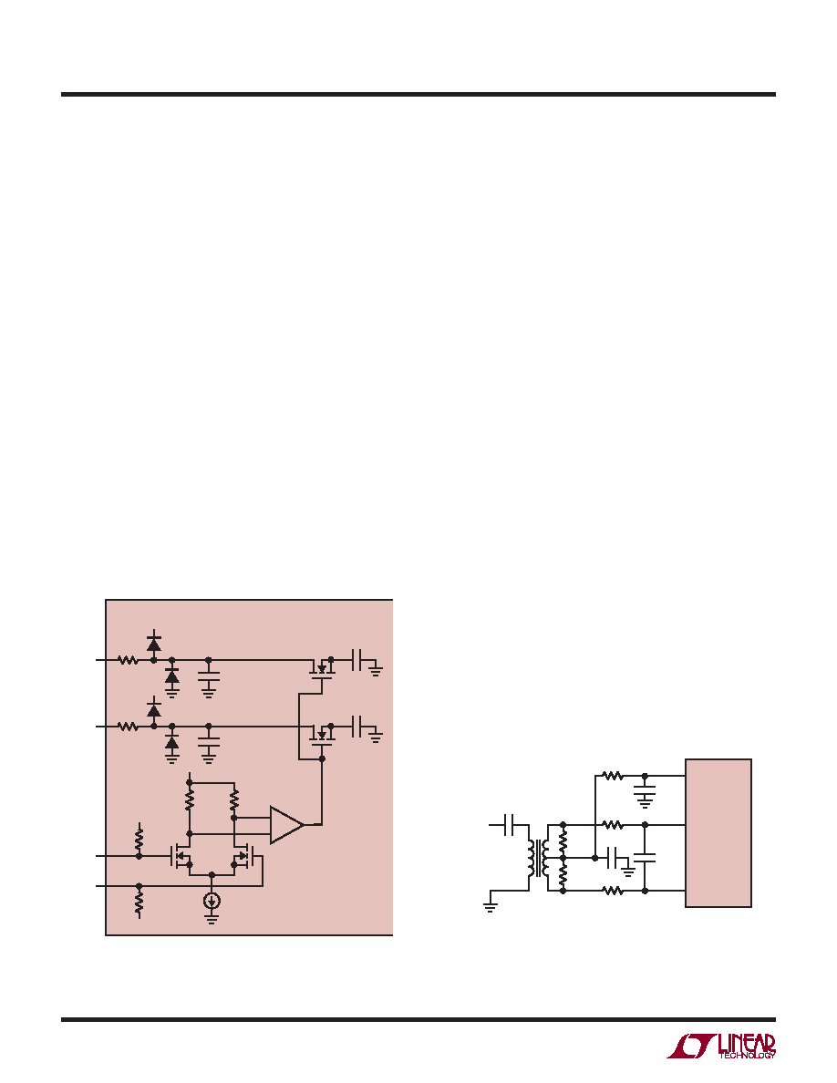
ANALOG INPUT
The analog inputs are differential CMOS sample-and-hold
circuits (Figure 2). The inputs should be driven differen-
tially around a common mode voltage set by the VCM1 or
VCM2 output pins, which are nominally VDD/2. For the 2V
input range, the inputs should swing from VCM – 0.5V
to VCM + 0.5V. There should be 180° phase difference
between the inputs.
The two channels are simultaneously sampled by a shared
encode circuit (Figure 2).
Single-Ended Input
For applications less sensitive to harmonic distortion, the
AIN+ input can be driven single-ended with a 1VP-P signal
centered around VCM. The AIN– input should be connected
to VCM and the VCM bypass capacitor should be increased
to 2.2μF. With a single-ended input, the harmonic distortion
and INL will degrade, but the noise and DNL will remain
unchanged.
INPUT DRIVE CIRCUITS
Input Filtering
If possible, there should be an RC lowpass filter right at
the analog inputs. This lowpass filter isolates the drive
circuitry from the A/D sample-and-hold switching, and
also limits wideband noise from the drive circuitry. Figure 3
shows an example of an input RC filter. The RC component
values should be chosen based on the application’s input
frequency.
Transformer Coupled Circuits
Figure 3 shows the analog input being driven by an RF
transformer with a center-tapped secondary. The center
tap is biased with VCM, setting the A/D input at its opti-
mal DC level. At higher input frequencies, a transmission
line balun transformer (Figure 4 to Figure 6) has better
balance, resulting in lower A/D distortion.
CSAMPLE
5pF
RON
15Ω
RON
15Ω
VDD
LTC2142
AIN
+
21421014 F02
CSAMPLE
5pF
VDD
AIN
–
ENC–
ENC+
1.2V
10k
1.2V
10k
CPARASITIC
1.8pF
CPARASITIC
1.8pF
10Ω
25Ω
50Ω
0.1μF
AIN
+
AIN
–
12pF
0.1μF
VCM
LTC2142
ANALOG
INPUT
0.1μF
T1
1:1
T1: MA/COM MABAES0060
RESISTORS, CAPACITORS
ARE 0402 PACKAGE SIZE
21421014 F03
Figure 2. Equivalent Input Circuit. Only One of
the Two Analog Channels Is Shown
Figure 3. Analog Input Circuit Using a Transformer.
Recommended for Input Frequencies from 5MHz to 70MHz
APPLICATIONS INFORMATION
相關PDF資料 |
PDF描述 |
|---|---|
| VX-53-1C23 | SWITCH LEVER SPDT 5A .187QC |
| 370 | T 1 3/4 18V .04 AMP LAMP |
| DC1620A-J | BOARD DEMO 65MSPS LTC2142-14 |
| 1850 | LAMP T3-1/4 MINI BAYONET BASE |
| 89 | LAMP INCAND G-6 S.C. BAYONET |
相關代理商/技術參數 |
參數描述 |
|---|---|
| DC1620A-L | 功能描述:BOARD DEMO 25MSPS LTC2140-14 RoHS:是 類別:未定義的類別 >> 其它 系列:* 標準包裝:1 系列:* 其它名稱:MS305720A |
| DC1620A-M | 功能描述:BOARD DEMO 125MSPS LTC2145-12 RoHS:是 類別:未定義的類別 >> 其它 系列:* 標準包裝:1 系列:* 其它名稱:MS305720A |
| DC1620A-N | 功能描述:BOARD DEMO 105MSPS LTC2144-12 RoHS:是 類別:未定義的類別 >> 其它 系列:* 標準包裝:1 系列:* 其它名稱:MS305720A |
| DC1620A-O | 功能描述:BOARD DEMO 80MSPS LTC2143-12 RoHS:是 類別:未定義的類別 >> 其它 系列:* 標準包裝:1 系列:* 其它名稱:MS305720A |
| DC1620A-P | 功能描述:BOARD DEMO 65MSPS LTC2142-12 RoHS:是 類別:未定義的類別 >> 其它 系列:* 標準包裝:1 系列:* 其它名稱:MS305720A |
發布緊急采購,3分鐘左右您將得到回復。