- 您現在的位置:買賣IC網 > PDF目錄376710 > DG444 (Intersil Corporation) Monolithic, Quad SPST, CMOS Analog Switches PDF資料下載
參數資料
| 型號: | DG444 |
| 廠商: | Intersil Corporation |
| 英文描述: | Monolithic, Quad SPST, CMOS Analog Switches |
| 中文描述: | 改進的四路、SPST模擬開關 |
| 文件頁數: | 6/10頁 |
| 文件大小: | 396K |
| 代理商: | DG444 |
D
Improved, Quad, SPST Analog Switches
6
_______________________________________________________________________________________
t
OFF
0.8 x V
OUT
V
OUT
0.8 x V
OUT
tf < 20ns
tr < 20ns
50%
0V
0V
+3V
SWITCH
OUTPUT
LOGIC INPUT WAVEFORM IS INVERTED FOR SWITCHES
THAT HAVE THE OPPOSITE LOGIC SENSE.
t
ON
SWITCH
INPUT
LOGIC
INPUT
+3V
IN
+5V
V-
-15V
( )
R
L
C
L
V
OUT
S
C
L
INCLUDES FIXTURE AND STRAY CAPACITANCE.
GND
REPEAT TEST FOR CHANNELS 2, 3, AND 4.
V
OUT
= V
D
L
LOGIC
INPUT
V
L
+15V
V+
D
DG444
DG445
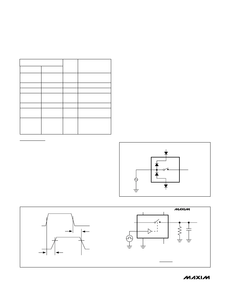
Figure 2. Switching Time
Applications Information
General Operation
Switches are open when power is off.
IN, D, and S should not exceed V+ or V-, even with
the power off.
Switch leakage is from each analog switch terminal
to V+ or V-, not to other switch terminals.
Operation with Supply Voltages
Other than ±15V
Using supply voltages other than ±15V will reduce the
analog signal range. The DG444/DG445 switches oper-
ate with ±4.5V to ±20V bipolar supplies or with a +10V
to +30V single supply; connect V- to 0V when operating
with a single supply. Also, all device types can operate
with unbalanced supplies such as +24V and -5V. V
L
must be connected to +5V to be TTL compatible, or to
V+ for CMOS-logic level inputs. The
Typical Operating
Characteristics
graphs show typical on-resistance with
±20V, ±15V, ±10V, and ±5V supplies. (Switching times
increase by a factor of two or more for operation at ±5V.)
Overvoltage Protection
Proper power-supply sequencing is recommended
for all CMOS devices. Do not exceed the absolute
maximum ratings because stresses beyond the list-
ed ratings may cause permanent damage to the
devices. Always sequence V+ on first, followed by
V
L
, V-, and logic inputs. If power-supply sequenc-
ing is not possible, add two small, external signal
diodes in series with supply pins for overvoltage
protection (Figure 1). Adding diodes reduces the
analog signal range to 1V below V+ and 1V above
V-, but low switch resistance and low leakage char-
acteristics are unaffected. Device operation is
unchanged, and the difference between V+ and V-
should not exceed +44V.
V+
D
V-
S
V
g
Figure 1. Overvoltage Protection Using External Blocking Diodes
_____________________Pin Description
13
12
5
4
3, 14, 11, 6
2, 15, 10, 7
1, 16, 9, 8
IN1–IN4
D1–D4
S1–S4
V-
GND
V
L
V+
Positive-Supply-
Voltage Input—
Connected to
Substrate
Logic-Supply
Voltage Input
Ground
Negative-Supply
Voltage Input
Source Outputs
Drain Outputs
Logic Control
Inputs
NAME
FUNCTION
11
10
3
2
1, 12, 9, 4
16, 13, 8, 5
15, 14, 7, 6
PIN
DIP/SO
QFN
相關PDF資料 |
PDF描述 |
|---|---|
| DG444DJ | Monolithic, Quad SPST, CMOS Analog Switches |
| DG444DY | Monolithic, Quad SPST, CMOS Analog Switches |
| DG458AK | 8-Channel Analog Multiplexer |
| DG459AK | 4-Channel Analog Multiplexer |
| DG458 | Fault-Protected Single 8-Ch/Differential 4-Ch Analog Multiplexers |
相關代理商/技術參數 |
參數描述 |
|---|---|
| DG444_06 | 制造商:INTERSIL 制造商全稱:Intersil Corporation 功能描述:Monolithic, Quad SPST, CMOS Analog Switches |
| DG444_07 | 制造商:INTERSIL 制造商全稱:Intersil Corporation 功能描述:Monolithic, Quad SPST, CMOS Analog Switches |
| DG444_11 | 制造商:VISHAY 制造商全稱:Vishay Siliconix 功能描述:Quad SPST CMOS Analog Switches |
| DG444AK | 制造商:未知廠家 制造商全稱:未知廠家 功能描述:SPST Analog Switch |
| DG444B | 制造商:VISHAY 制造商全稱:Vishay Siliconix 功能描述:Improved Quad SPST CMOS Analog Switches |
發布緊急采購,3分鐘左右您將得到回復。