- 您現在的位置:買賣IC網 > PDF目錄21322 > DSPIC33FJ128GP202T-I/MM (Microchip Technology)IC DSPIC MCU/DSP 128K 28-QFN PDF資料下載
參數資料
| 型號: | DSPIC33FJ128GP202T-I/MM |
| 廠商: | Microchip Technology |
| 文件頁數: | 69/73頁 |
| 文件大小: | 0K |
| 描述: | IC DSPIC MCU/DSP 128K 28-QFN |
| 標準包裝: | 1,600 |
| 系列: | dsPIC™ 33F |
| 核心處理器: | dsPIC |
| 芯體尺寸: | 16-位 |
| 速度: | 40 MIP |
| 連通性: | I²C,IrDA,LIN,SPI,UART/USART |
| 外圍設備: | AC'97,欠壓檢測/復位,DMA,I²S,POR,PWM,WDT |
| 輸入/輸出數: | 21 |
| 程序存儲器容量: | 128KB(128K x 8) |
| 程序存儲器類型: | 閃存 |
| RAM 容量: | 8K x 8 |
| 電壓 - 電源 (Vcc/Vdd): | 3 V ~ 3.6 V |
| 數據轉換器: | A/D 10x10b/12b |
| 振蕩器型: | 內部 |
| 工作溫度: | -40°C ~ 85°C |
| 封裝/外殼: | 28-VQFN 裸露焊盤 |
| 包裝: | 帶卷 (TR) |
| 配用: | DV164033-ND - KIT START EXPLORER 16 MPLAB ICD2 DM240001-ND - BOARD DEMO PIC24/DSPIC33/PIC32 |
第1頁第2頁第3頁第4頁第5頁第6頁第7頁第8頁第9頁第10頁第11頁第12頁第13頁第14頁第15頁第16頁第17頁第18頁第19頁第20頁第21頁第22頁第23頁第24頁第25頁第26頁第27頁第28頁第29頁第30頁第31頁第32頁第33頁第34頁第35頁第36頁第37頁第38頁第39頁第40頁第41頁第42頁第43頁第44頁第45頁第46頁第47頁第48頁第49頁第50頁第51頁第52頁第53頁第54頁第55頁第56頁第57頁第58頁第59頁第60頁第61頁第62頁第63頁第64頁第65頁第66頁第67頁第68頁當前第69頁第70頁第71頁第72頁第73頁
2007-2012 Microchip Technology Inc.
DS70292G-page 71
dsPIC33FJ32GP302/304, dsPIC33FJ64GPX02/X04, AND dsPIC33FJ128GPX02/X04
5.0
FLASH PROGRAM MEMORY
The dsPIC33FJ32GP302/304, dsPIC33FJ64GPX02/
X04, and dsPIC33FJ128GPX02/X04 devices contain
internal Flash program memory for storing and
executing application code. The memory is readable,
writable and erasable during normal operation over the
entire VDD range.
Flash memory can be programmed in two ways:
In-Circuit Serial Programming (ICSP)
programming capability
Run-Time Self-Programming (RTSP)
ICSP
allows
any
of
the
following
devices,
dsPIC33FJ32GP302/304, dsPIC33FJ64GPX02/X04,
and
dsPIC33FJ128GPX02/X04,
to
be
serially
programmed while in the end application circuit. This is
done with two lines for programming clock and
programming data (one of the alternate programming
pin pairs: PGECx/PGEDx), and three other lines for
power (VDD), ground (VSS) and Master Clear (MCLR).
This allows customers to manufacture boards with
unprogrammed devices and then program the digital
signal controller just before shipping the product. This
also allows the most recent firmware or a custom
firmware to be programmed.
RTSP is accomplished using TBLRD (table read) and
TBLWT (table write) instructions. With RTSP, the user
application can write program memory data either in
blocks or ‘rows’ of 64 instructions (192 bytes) at a time
or a single program memory word, and erase program
memory in blocks or ‘pages’ of 512 instructions (1536
bytes) at a time.
5.1
Table Instructions and Flash
Programming
Regardless of the method used, all programming of
Flash memory is done with the table read and table
write instructions. These allow direct read and write
access to the program memory space from the data
memory while the device is in normal operating mode.
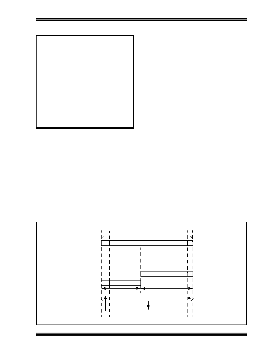
The 24-bit target address in the program memory is
formed using bits <7:0> of the TBLPAG register and the
Effective Address (EA) from a W register specified in
the table instruction, as shown in Figure 5-1.
The TBLRDL and the TBLWTL instructions are used to
read or write to bits <15:0> of program memory.
TBLRDL and TBLWTL can access program memory in
both Word and Byte modes.
The TBLRDH and TBLWTH instructions are used to read
or write to bits <23:16> of program memory. TBLRDH
and TBLWTH can also access program memory in Word
or Byte mode.
FIGURE 5-1:
ADDRESSING FOR TABLE REGISTERS
Note 1: This data sheet summarizes the features
of
the
dsPIC33FJ32GP302/304,
dsPIC33FJ64GPX02/X04,
and
dsPIC33FJ128GPX02/X04 families of
devices. It is not intended to be a
comprehensive reference source. To
complement the information in this data
sheet, refer to Section 5. “Flash
Programming”
(DS70191)
of
the
“dsPIC33F/PIC24H Family Reference
Manual”, which is available from the
Microchip website (www.microchip.com).
2: Some registers and associated bits
described in this section may not be avail-
able on all devices. Refer to Section 4.0
“Memory Organization” in this data
sheet for device-specific register and bit
information.
0
Program Counter
24 bits
Program Counter
TBLPAG Reg
8 bits
Working Reg EA
16 bits
Byte
24-bit EA
0
1/0
Select
Using
Table Instruction
Using
User/Configuration
Space Select
相關PDF資料 |
PDF描述 |
|---|---|
| P51-1500-A-Z-D-4.5OVP-000-000 | SENSOR 1500PSI 1/4-18NPT .5-4.5V |
| REC8-4815SRWZ/H3/A/M | CONV DC/DC 8W 48VIN 15VOUT |
| 70-ODC5 | OUTPUT MODULE DC STD 14MA 5VDC |
| REC3.5-1224SRW/R8/A/CTRL | CONV DC/DC 3.5W 9-18VIN 24VOUT |
| P51-100-S-O-P-20MA-000-000 | SENSOR 100PSIS 7/16 UNF 4-20MA |
相關代理商/技術參數 |
參數描述 |
|---|---|
| dsPIC33FJ128GP204-E/ML | 功能描述:數字信號處理器和控制器 - DSP, DSC 16b DSC 128KB Flash DMA 40MIPS RoHS:否 制造商:Microchip Technology 核心:dsPIC 數據總線寬度:16 bit 程序存儲器大小:16 KB 數據 RAM 大小:2 KB 最大時鐘頻率:40 MHz 可編程輸入/輸出端數量:35 定時器數量:3 設備每秒兆指令數:50 MIPs 工作電源電壓:3.3 V 最大工作溫度:+ 85 C 封裝 / 箱體:TQFP-44 安裝風格:SMD/SMT |
| dsPIC33FJ128GP204-E/PT | 功能描述:數字信號處理器和控制器 - DSP, DSC 16b DSC 128KB Flash DMA 40MIPS RoHS:否 制造商:Microchip Technology 核心:dsPIC 數據總線寬度:16 bit 程序存儲器大小:16 KB 數據 RAM 大小:2 KB 最大時鐘頻率:40 MHz 可編程輸入/輸出端數量:35 定時器數量:3 設備每秒兆指令數:50 MIPs 工作電源電壓:3.3 V 最大工作溫度:+ 85 C 封裝 / 箱體:TQFP-44 安裝風格:SMD/SMT |
| dsPIC33FJ128GP204-I/ML | 功能描述:數字信號處理器和控制器 - DSP, DSC 16B DSC 44LD128KB DMA 40MIPS RoHS:否 制造商:Microchip Technology 核心:dsPIC 數據總線寬度:16 bit 程序存儲器大小:16 KB 數據 RAM 大小:2 KB 最大時鐘頻率:40 MHz 可編程輸入/輸出端數量:35 定時器數量:3 設備每秒兆指令數:50 MIPs 工作電源電壓:3.3 V 最大工作溫度:+ 85 C 封裝 / 箱體:TQFP-44 安裝風格:SMD/SMT |
| dsPIC33FJ128GP204-I/PT | 功能描述:數字信號處理器和控制器 - DSP, DSC 16B DSC 128KB DMA 40MIPS RoHS:否 制造商:Microchip Technology 核心:dsPIC 數據總線寬度:16 bit 程序存儲器大小:16 KB 數據 RAM 大小:2 KB 最大時鐘頻率:40 MHz 可編程輸入/輸出端數量:35 定時器數量:3 設備每秒兆指令數:50 MIPs 工作電源電壓:3.3 V 最大工作溫度:+ 85 C 封裝 / 箱體:TQFP-44 安裝風格:SMD/SMT |
| dsPIC33FJ128GP204T-I/ML | 功能描述:數字信號處理器和控制器 - DSP, DSC 16B DSC 44LD128KB DMA 40MIPS RoHS:否 制造商:Microchip Technology 核心:dsPIC 數據總線寬度:16 bit 程序存儲器大小:16 KB 數據 RAM 大小:2 KB 最大時鐘頻率:40 MHz 可編程輸入/輸出端數量:35 定時器數量:3 設備每秒兆指令數:50 MIPs 工作電源電壓:3.3 V 最大工作溫度:+ 85 C 封裝 / 箱體:TQFP-44 安裝風格:SMD/SMT |
發布緊急采購,3分鐘左右您將得到回復。