- 您現在的位置:買賣IC網 > PDF目錄377020 > DTA1C (Sanyo Electric Co.,Ltd.) 1.0A Bidirectional Thyristor PDF資料下載
參數資料
| 型號: | DTA1C |
| 廠商: | Sanyo Electric Co.,Ltd. |
| 英文描述: | 1.0A Bidirectional Thyristor |
| 中文描述: | 安培雙向晶閘管 |
| 文件頁數: | 1/3頁 |
| 文件大小: | 165K |
| 代理商: | DTA1C |
DTA1
Ordering number : EN2283B
1.0A Bidirectional Thyristor
Silicon Planar Type
SANYO Electric Co.,Ltd. Semiconductor Bussiness Headquarters
TOKYO OFFICE Tokyo Bldg., 1-10, 1 Chome, Ueno, Taito-ku, TOKYO, 110 JAPAN
O0797GI/3089MO, TS No.2283-1/3
Features
Low AC power control use.
Peak OFF-state voltage : 200 to 400V
RMS ON-state current : 1A
TO-92 package.
Absolute Maximum Ratings
at Ta=25°C
Repetitive Peak
OFF-StateVoltage
RMS ON-State Current
DTA1C
DTA1E
unit
V
V
DRM
200
400
I
T(RMS)
Tc=74°C, single-phase
full-wave
Peak 1 cycle, 50Hz
1ms
≤
t
≤
10ms
f
≥
50Hz, duty
≤
10%
→
1.0
A
Surge ON-State Current
Amperes Squared-Seconds
Peak Gate Power Dissipation
Average Gate Power Dissipation
Peak Gate Current
Peak Gate Voltage
Junction Temperature
Strage Temperature
Weght
I
TSM
∫
i
2
T·dt
P
GM
P
G(AV)
I
GM
V
GM
Tj
Tstg
→
→
→
→
→
→
→
8
A
A
2
s
W
W
A
V
°C
°C
g
0.32
1
0.1
±0.5
±6
125
f
≥
50Hz, duty
≤
10%
f
≥
50Hz, duty
≤
10%
–40 to +125
→
0.2
Electrical Characteristics
at Ta=25°C
Repetitive Peak
OFF-State Current
Peak ON-State Voltage
Holding Current
Gate Trigger Current* (I)
min
typ
max
10
unit
μA
I
DRM
Tj=25°C, V
D
=V
DRM
V
TM
I
H
I
GT
I
GT
I
GT
I
GT
V
GT
V
GT
V
GT
V
GT
V
GD
Rth(j-c)
I
TM
=1.5A
V
D
=12V, gate open
V
D
=12V, R
L
=20
V
D
=12V, R
L
=20
V
D
=12V, R
L
=20
V
D
=12V, R
L
=20
V
D
=12V, R
L
=20
V
D
=12V, R
L
=20
V
D
=12V, R
L
=20
V
D
=12V, R
L
=20
Tc=125°C, V
D
=V
DRM
Between junction and case, AC
1.5
10
V
mA
mA
mA
mA
mA
V
V
V
V
V
°C/W
5
5
(II)
(III)
(IV)
10
5
2
2
–
2
–
Gate Trigger Voltage* (I)
(II)
(III)
(IV)
2
Gate Nontrigger Voltage
Thermal Resistance
0.2
40
* : The gate trigger mode is shown below.
Trigger mode
I
II
III
IV
T2
+
+
–
–
T1
–
–
+
+
G
+
–
+
–
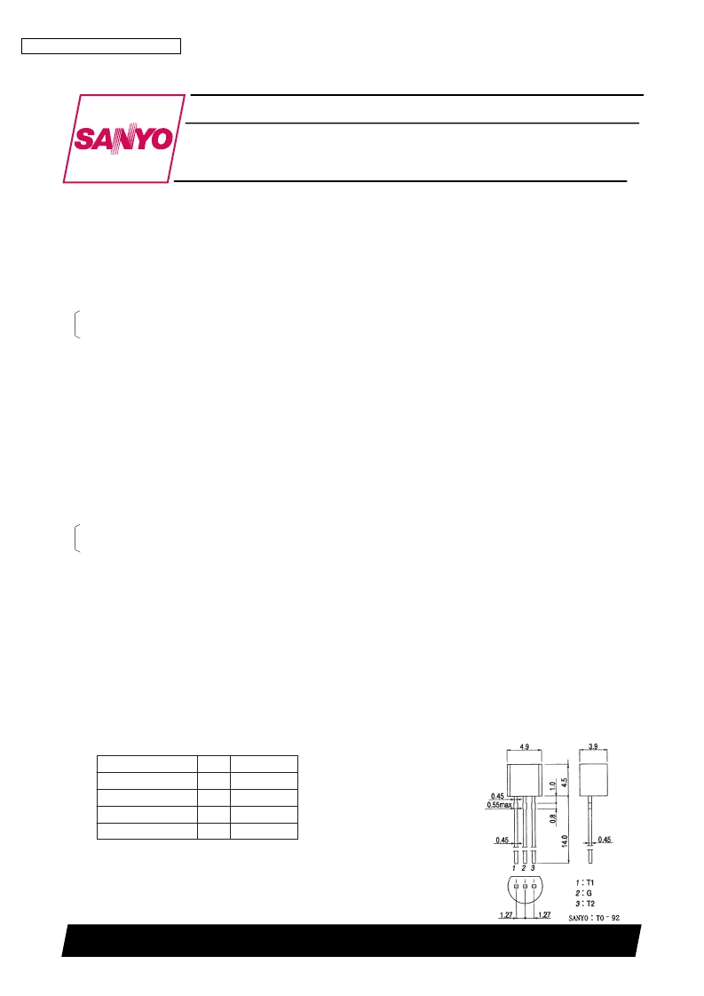
Package Dimensions
1192B
(unit : mm)
相關PDF資料 |
PDF描述 |
|---|---|
| DTA1E | 1.0A Bidirectional Thyristor |
| DTA2B | 2.0A Bidirectional Thyristor |
| DTA2C | 2.0A Bidirectional Thyristor |
| DTA2E | MOSFET N-CH 200V 5A TO-220FN |
| DTA2 | |
相關代理商/技術參數 |
參數描述 |
|---|---|
| DTA2 | 制造商:SANYO 制造商全稱:Sanyo Semicon Device 功能描述:2.0A Bidirectional Thyristor |
| DTA214YA | 制造商:未知廠家 制造商全稱:未知廠家 功能描述:TRANSISTOR | 50V V(BR)CEO | 100MA I(C) | SIP |
| DTA214YAA | 制造商:未知廠家 制造商全稱:未知廠家 功能描述:TRANSISTOR | 50V V(BR)CEO | 100MA I(C) | SC-71 |
| DTA214YC | 制造商:未知廠家 制造商全稱:未知廠家 功能描述:TRANSISTOR | 50V V(BR)CEO | 70MA I(C) | SOT-23 |
| DTA214YCA | 制造商:未知廠家 制造商全稱:未知廠家 功能描述:TRANSISTOR | 50V V(BR)CEO | 100MA I(C) | SOT-23 |
發布緊急采購,3分鐘左右您將得到回復。